Light emission device and display device using the light emission device as light source

a technology of light emission device and light emission surface, which is applied in the manufacture of electrode systems, electric discharge tubes/lamps, instruments, etc., can solve the problems of low high-voltage stability, unintentional electron emission of anodes, and possible diodes, so as to improve the luminance of a light emission surface and increase high-voltage stability

Inactive Publication Date: 2009-01-08
SAMSUNG SDI CO LTD
View PDF13 Cites 2 Cited by
  • Summary
  • Abstract
  • Description
  • Claims
  • Application Information

AI Technical Summary

Benefits of technology

[0011]Exemplary embodiments provide a light emission device having advantages of suppressing arc discharge by increasing high voltage stability and of...

Problems solved by technology

However, since the electron emission regions are directly influenced by an anode electric field in the light emission device, the anode electric field around the electron emission regions is strengthened as the anode voltage increases, and diode emission may occur, in which the anode electric field unintentionally emits electro...

Method used


Image

  • Light emission device and display device using the light emission device as light source
  • Light emission device and display device using the light emission device as light source
  • Light emission device and display device using the light emission device as light source

Examples


Embodiment Construction

[0045]Certain embodiments will now be described more fully with reference to the accompanying drawings, in which exemplary embodiments are shown, which, however, may be embodied in many different forms and should not be construed as being limited to the embodiments set forth herein. Rather these embodiments are provided so that this disclosure will be thorough and complete, and will fully convey the concept to those skilled in the art.

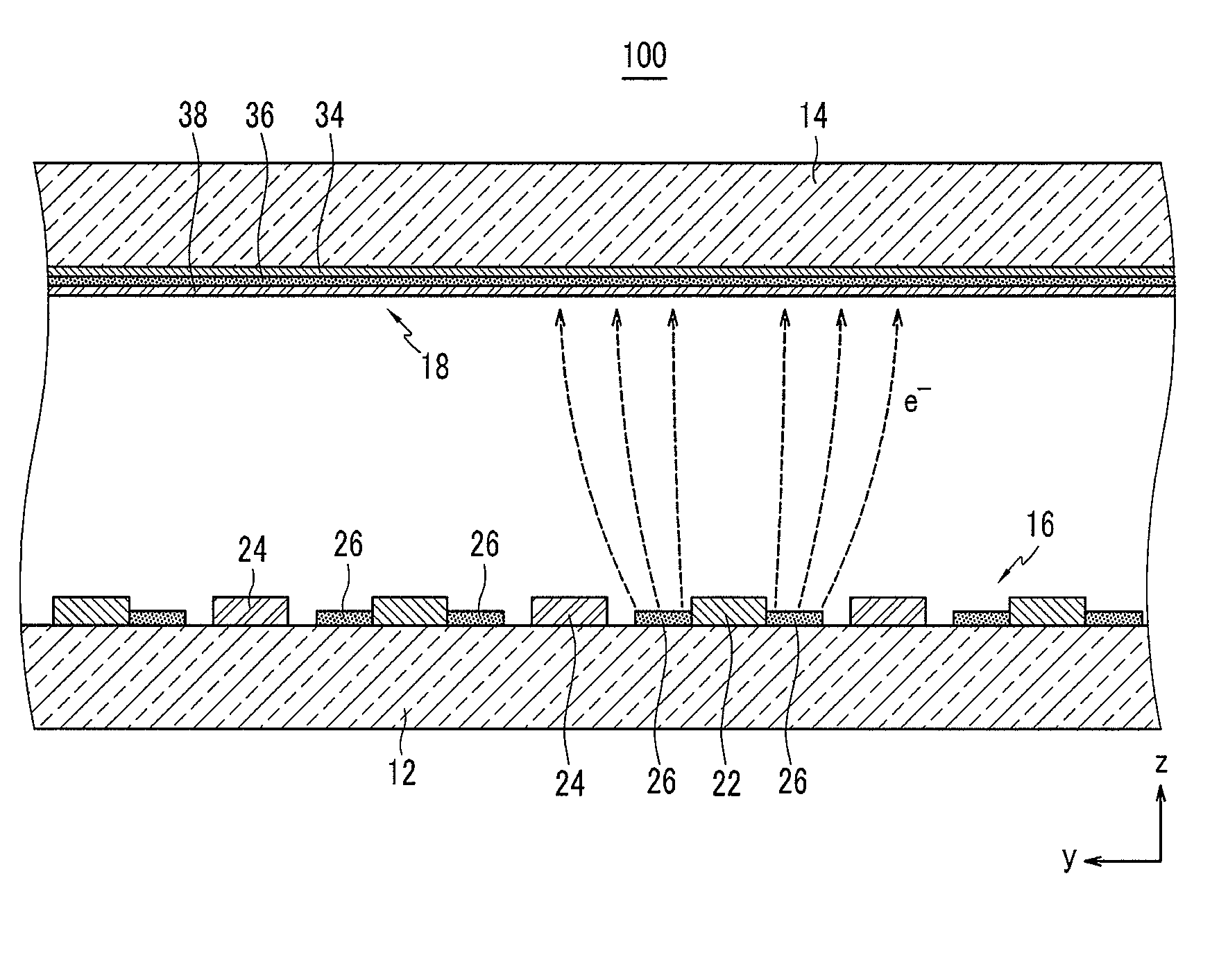
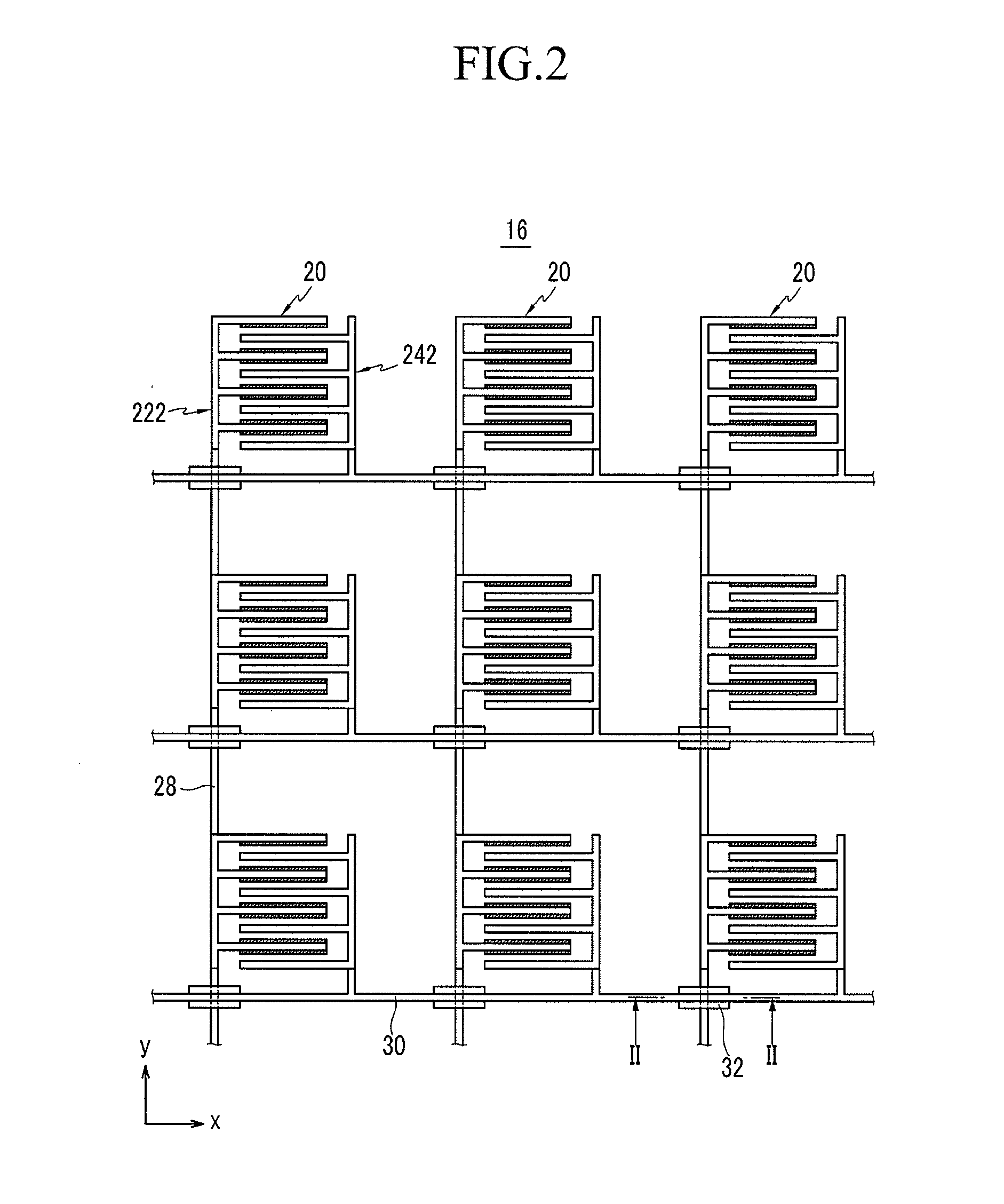
[0046]A light emission device according to a first exemplary embodiment of the present invention will be described with reference to FIGS. 1 to 4.

[0047]Referring to FIG. 1 to FIG. 3, the light emission device 100 of the present exemplary embodiment includes the first substrate 12 and the second substrate 14, which are arranged opposite to each other in parallel with a predetermined gap therebetween. The first and second substrates 12 and 14 are sealed together along their peripheries with a sealing member (not shown), and the inner space therebetween i...


PUM


Abstract

A light emission device for improving high voltage stability and a display device using the same as a light source includes first and second substrates facing each other, an electron emission unit located on one side of the first substrate and including a plurality of electron emission elements, and a light emission unit located on one side of the second substrate and emitting a visible light. Each of the electron emission elements includes first electrodes spaced apart from each other by a predetermined interval along a first direction of the first substrate, second electrodes arranged between the first electrodes along the first direction, and first electron emission regions electrically connected to the first electrodes and formed at a predetermined height lower than that of the first electrodes.

Description

CROSS-REFERENCE TO RELATED APPLICATION[0001]This application claims priority to and the benefit of Korean Patent Application No. 10-2007-0066582, filed in the Korean Intellectual Property Office on Jul. 3, 2007, the entire contents of which is incorporated herein by reference.BACKGROUND[0002]1. Technical Field[0003]The present disclosure relates to a light emission device, more particularly, to a light emission device with an improved structure of an electron emission unit and a display device using the light emission unit as its light source.[0004]2. Description of the Related Art[0005]There are many different types of light emission devices that radiate visible light. One type of light emission device includes a structure in which a phosphor layer and an anode electrode are disposed on a front substrate, and electron emission regions and driving electrodes are disposed on a rear substrate. The front and rear substrates are sealed to each other at their peripheries using a sealing ...

Claims


Application Information

Patent Timeline
IPC IPC(8): G02F1/13357H01J1/88
CPCG02F1/133602H01J63/06H01J63/02G02F2001/133625G02F1/133625H01J1/304H01J9/32
Inventor KIM, YOON-JINKIM, JAE-MYUNGJOO, KYU-NAMPARK, HYUN-KICHO, YOUNG-SUKMOON, HEE-SUNGLEE, SO-RA
Owner SAMSUNG SDI CO LTD
Why Eureka
Try Eureka