


Quick Research
Generate reliable direction feasibility study reports for your R&D in just a few steps.

Technical Q&A
Discover and master advanced knowledge NOW. Basics, ideas, possibilities, all at once.

Find Solutions
As an expert in R&D theories, this can generate solutions to your technical problems instantly.

Evaluate Feasibility
Analyze your overall solution with one click, know your potential R&D risks in advance.

Monitor Landscape
Get weekly tech updates, stay abreast of the latest tech innovations and key insights.
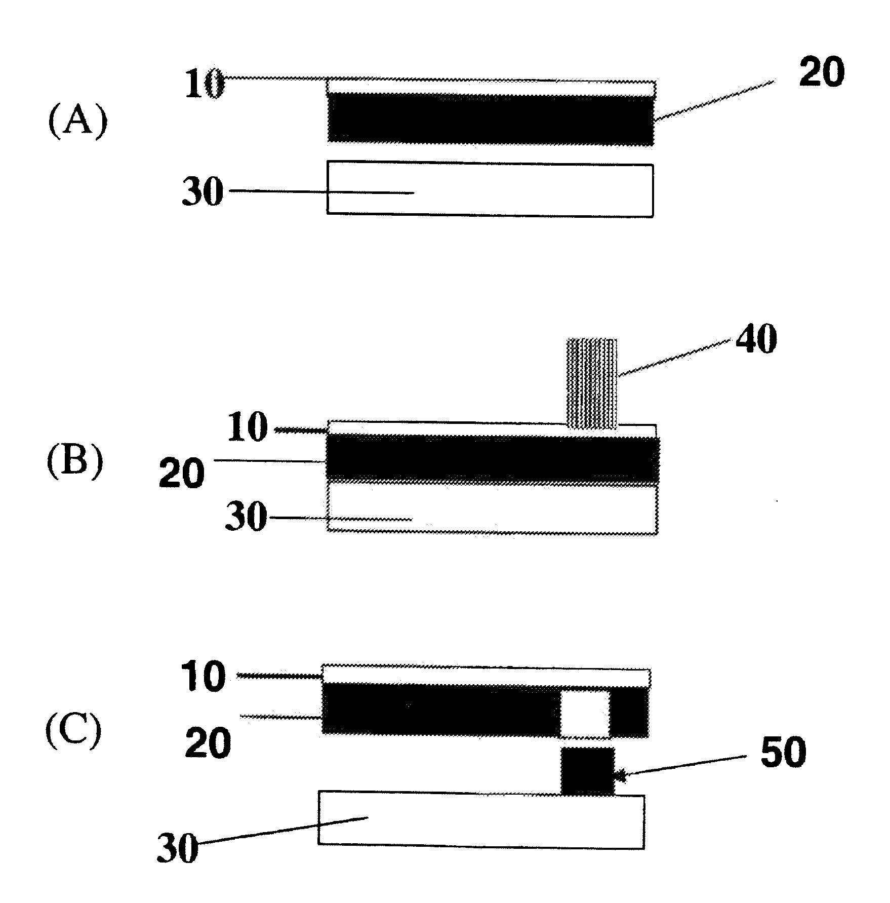
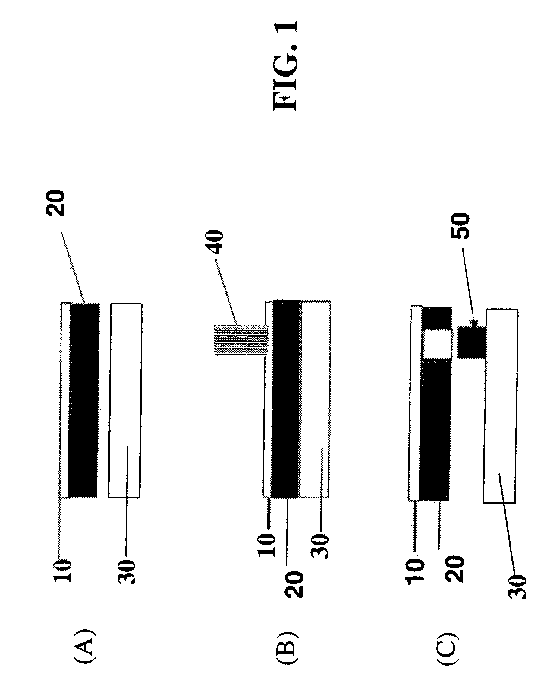
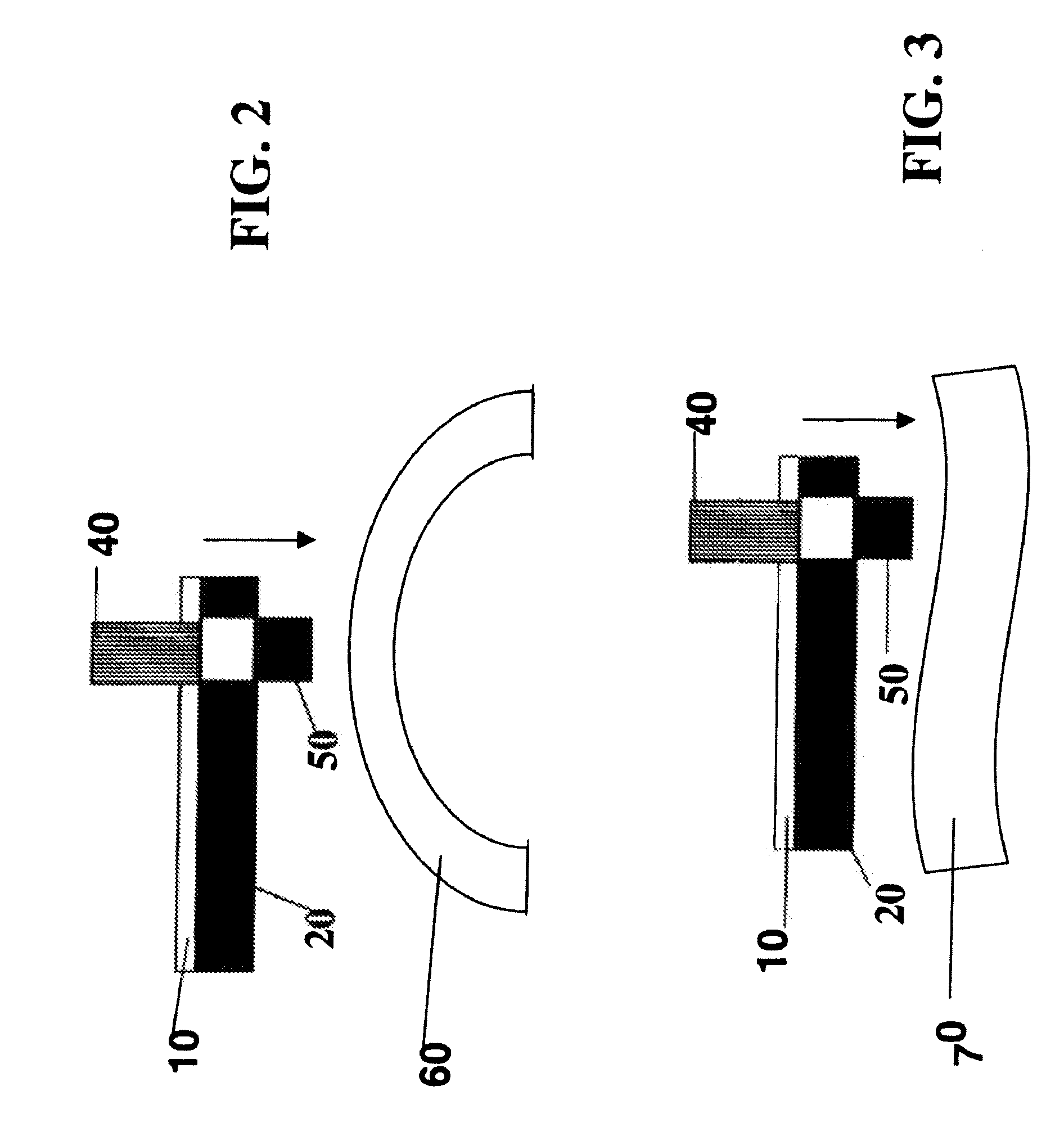
Laser transfer articles and method of making
a technology of laser transfer and transfer articles, applied in the field of semiconductor and electronics industries, can solve the problems of not being well suited to the transfer of organic materials, requiring special equipment, and becoming more reactive, etc., and achieves the effect of facilitating liquid-free transfer of high-performance devices and higher performan
- Summary
- Abstract
- Description
- Claims
- Application Information
AI Technical Summary
Benefits of technology
Problems solved by technology
Method used
Image

Examples
example 1
[0080]This example illustrates transfer of silicon from a first substrate to a second substrate using embodiments of the method and apparatus of this invention. Two laser systems were used. Laser system A was an ESI model 44 laser trimming station. This system had a beam collimating optic that reduce the spot size by 50%. Laser B was an AB laser LBI6000 laser marking system (a multimode laser). Both systems used Q switched Nd:YAG lasers (fundamental). Power measurements were taken using an Ophia Orion TH power meter. Both laser systems had XY translation stages. On system A the Q switch was run at 100 Hz and the stage speed was set at 10 inch / min (6 mm / s) so that the spot separation would be 60 μm. For system B, the Q switch was fired at 100 Hz, but the translation speed was set at 1.2 inch / sec (30.5 mm / s) which would give a spot separation of 305 μm. For experiments 1-5, a 3M transparency film was used as the receiving substrate, for experiments 6-7 glass was the receiving substrat...
example 2
[0081]This example describes transferring silicon from a glass substrate to a second substrate. The maximum energy of a laser pulse that can pass through the donor substrate is first determined. This is a function of how much of the pulse energy is absorbed by the substrate. A substrate that may be used is a 4×4×0.06 inch soda lime glass substrate available from Nanofilm (LOT#0327033). A piece of this glass can be spectroscopically analyzed and undergo zap testing with pulsed YAG lasers at λ-1064 nm and λ-335 nm and if necessary at frequency doubled λ-532 nm to determine its absorption characteristics.
[0082]The substrates may be coated with 0.1 μm to about 50 μm of Si. These silicon films could be sandwiched with an uncoated substrate and a piece of transparency film using 3M Spray Mount artist's adhesive. Initially the spot size of the laser will be set as small as possible; ideally a 10-25 μm spot will be used and the size of the spot may be increased up to 100 μm.
[0083]The sandwi...
example 3
[0085]Thin, 20-μm-thick silicon wafers were obtained from Virginia Semiconductor, Inc. (Fredericksburg, Va.) and mounted onto 0.090″-thick, 4″×4″ square quartz plates for photopatterning. Universal Photonics Unibond 5.0 adhesive wax was applied at each wafer's periphery to hold the wafer in place on the quartz plate. Photoresist was coated onto each wafer by spin-coating, exposed through a photomask, and developed at Micrometrics, Inc. (Londonderry, N.H.). Plasma etching of the silicon wafers resulted in the formation of 1″×2″ regions of 150-μm square silicon “mesas”. Each mesa was separated from the others by >20-μm wide channels each ≧10 μm deep. These dimensions were measured by scanning electron microscopy at Severn Trent Laboratories (Billerica, Mass.). The photopatterning process resulted in a 20-30% yield of 150-μm silicon squares. Thus patterned, each silicon wafer was then covered over with a 0.060″-thick, 4″×4″ soda lime glass substrate, leaving the etched wafers “sandwic...
PUM
| Property | Measurement | Unit |
|---|---|---|
| thickness | aaaaa | aaaaa |
| thickness | aaaaa | aaaaa |
| thickness | aaaaa | aaaaa |
Abstract
Description
Claims
Application Information
 - R&D Engineer
- R&D Manager
- IP Professional
- Industry Leading Data Capabilities
- Powerful AI technology
- Patent DNA Extraction
Browse by: Latest US Patents, China's latest patents, Technical Efficacy Thesaurus, Application Domain, Technology Topic, Popular Technical Reports.
© 2024 PatSnap. All rights reserved.Legal|Privacy policy|Modern Slavery Act Transparency Statement|Sitemap|About US| Contact US: help@patsnap.com