Multi-layer substrate and manufacturing method thereof

Active Publication Date: 2008-12-25
PRINCO CORP
View PDF23 Cites 8 Cited by
  • Summary
  • Abstract
  • Description
  • Claims
  • Application Information

AI Technical Summary

Benefits of technology

[0017]Another objective of the present invention is to provide a manufacturing method of a multi-layer substrate and the multi-layer substrate takes fewer processes, fewer materials and has greatly thin dielectric layers. Following concern of impedance matching, the metal line of the multi-layer substrate can keep good signal integrity therein.
[0019]According to the manufacturing method of the present invention, the thickness of the dielectric layer can be greatly reduced than the dielectric layer of the prior arts. Comparing with the 8-layer substrate products which's thickness is about 600 μm, one single layer thickness of the multi-layer substrate according to the present invention can reach below 10 μm and the thickness of an 8-layer substrate product can be about 80˜90 μm, and even thinner. Moreover, the present invention not only shrinks the size of the multi-layer substrate but also satisfies concern of impedance matching due to the greatly thin dielectric layer. Furthermore, crosstalk influence can be reduced when the high-frequency signal is transmitted through a Stripline. The present invention can keep good signal integrity and increase layout density.

Problems solved by technology

Moreover, due to complication of modern circuit design, many necessary detail processes coming up with, such as drilling, plating via or hole, etching, cleaning, polishing, black oxidizing and etc.
Therefore, one process failure can cause the whole multi-layer substrate to breakdown and decrease the yield thereof.
It's not easy to control the process quality and the manufacture cost because too many materials are being used.
Besides, miniaturization for electronic productions is an unavoidable trend in this modern world.
The aforesaid multi-layer substrate manufactured by hot pressing and adhering has limitation of trace pattern for size minimization.
Because the materials of the core and prepreg are composite materials, there are problems of difficult matching for the electric characteristic (such as Dk, dielectric constant) and mechanical characteristic (such as CTE, coefficient of expansion).
Then, the signal transmitted in one metal line can be easily interfered by the signal transmitted in the adjacent metal line.
The electric fields and performances of the signals transmitted in the adjacent metal lines interfere with each other and cause serious problems of the signal integrity, such as, crosstalk when high-frequency signals are transmitted through a stripline, high frequency noise and backward coupling caused by parasitic inductance and parasitic capacitor of the vias.
Many different materials employed in the prior arts result in difficulty of the mechanical characteristic matching.
The end product of the multi-layer substrate according to prior arts is thicker and losses the expected flexibility.

Method used


Image

  • Multi-layer substrate and manufacturing method thereof
  • Multi-layer substrate and manufacturing method thereof
  • Multi-layer substrate and manufacturing method thereof

Examples


Embodiment Construction

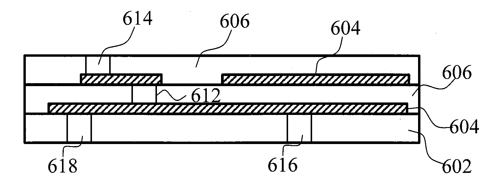
[0026]Please refer to FIG. 6A to FIG. 6D, which depict a structural flowchart of a manufacturing method according to the present invention. FIG. 6A shows steps of providing a carrier 600 and coating a first dielectric layer 602 on the carrier. FIG. 6B shows steps of forming a metal structure layer 604 on the first dielectric layer 602, proceeding a patterning process thereon, and then forming a second dielectric layer 606 on the metal structure layer 604, making a via 612 in the second dielectric layer 606. FIG. 6C shows steps of forming another metal structure layer 604 on the second dielectric layer 606, proceeding a patterning process thereon, and then forming another second dielectric layer 606 on the aforesaid metal structure layer 604, making a via 614 in the aforesaid second dielectric layer 606. Then, a multi-layer substrate is formed on the carrier 600. FIG. 6D shows a step of separating the multi-layer substrate from the carrier 600 to accomplish manufacturing the multi-la...


PUM

PropertyMeasurementUnit
Thicknessaaaaaaaaaa
Dielectric polarization enthalpyaaaaaaaaaa
Adhesion strengthaaaaaaaaaa

Abstract

Disclosed are a multi-layer substrate and a manufacturing method of the multi-layer substrate. By employing a carrier to alternately form dielectric layers and metal structure layers thereon. Each dielectric layer adheres with the adjacent dielectric layer to embed the metal structure layers in the dielectric layers corresponding thereto. Comparing with prior arts, which have to use prepregs when hot pressing and adhering different layers of different materials, the present invention takes fewer processes, thus, fewer kinds of materials without using prepregs. Therefore, the present invention can promote the entire quality and yield of manufacturing the multi-layer substrate to satisfy mechanical characteristic matching of the multi-layer substrate and to reduce cost of the whole manufacturing process. Significantly, the multi-layer substrate having thin dielectric layers according to the present invention can satisfy the concern of impedance matching therefore, and can reduce crosstalk influence to keep good signal integrity therein.

Description

BACKGROUND OF THE INVENTION[0001]1. Field of the Invention[0002]The present invention generally relates to a multi-layer substrate and manufacturing method thereof, and more particularly to a flexible multi-layer substrate and manufacturing method thereof.[0003]2. Description of Prior Art[0004]Please refer to FIG. 1, which depicts a diagram of multi-layer substrate manufactured by hot pressing and adhering different layers according to prior art. Basically, a multi-layer substrate that is manufactured by hot pressing and adhering is called Sequential Lamination from double side according to prior arts. First, a core 100 with copper clad 102 is provided. A lithography process and a development process are proceeded to the copper clad 102 to form pattern thereon (as being a metal structure layer, i.e. metal lines for transmitting signals). Then, laminating a prepreg 104, another core 100 which already had the metal structure layer 102 and another prepreg 104 laminated onto, and so on....

Claims


Application Information

Patent Timeline
IPC IPC(8): H05K1/02H05K3/38
CPCH05K3/0058Y10T29/49156H05K3/381H05K3/4682H05K2201/0154H05K2203/016H05K2203/065H05K2203/0759H05K2203/095Y10T29/49165Y10T29/4913Y10T29/49128Y10T29/49155Y10T29/49126H05K3/28
Inventor YANG, CHIH-KUANGCHANG, CHENG-YI
Owner PRINCO CORP
Why Eureka
Try Eureka