
Structure of tag integrated circuit flexible board

a flexible circuit board and integrated circuit technology, applied in the direction of printed circuit non-printed electric components association, semiconductor/solid-state device details, transportation and packaging, etc., can solve the problems of smd electronic components and the circuits on the circuit board may fall off, the base, pins and lenses of the light-emitting diodes may get damaged or contaminated by dirt on the ground, etc., to avoid the possible damage of electronic elements and be convenient to carry or transport.

Inactive Publication Date: 2008-12-18
PYROSWIFT HOLDING CO LIMITED
View PDF3 Cites 0 Cited by
  • Summary
  • Abstract
  • Description
  • Claims
  • Application Information

AI Technical Summary

Benefits of technology

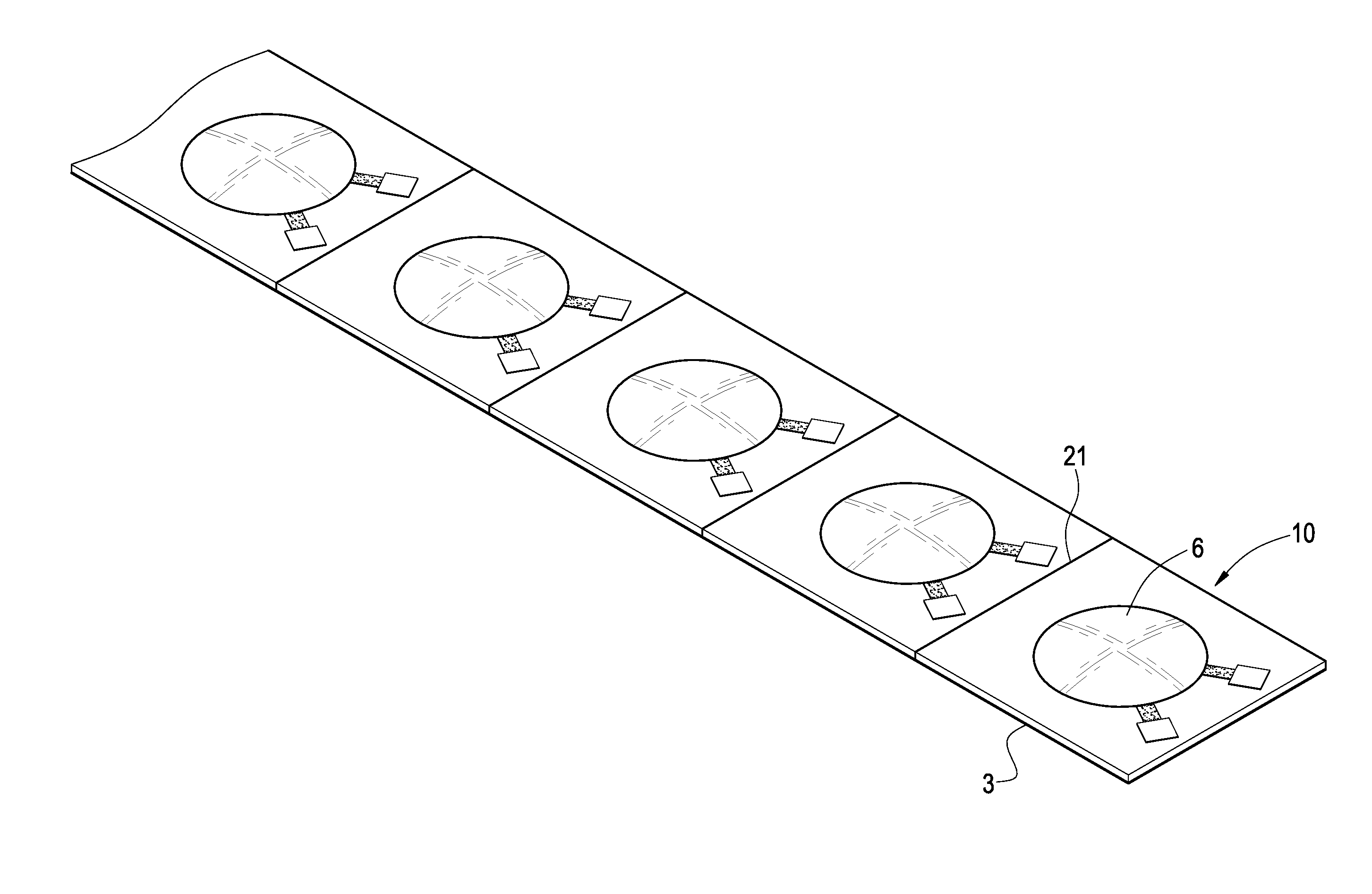
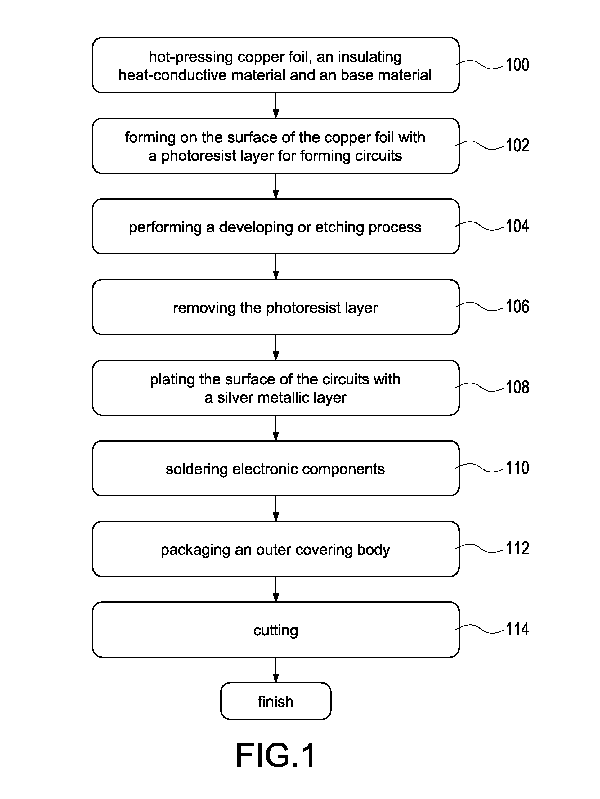
"The present invention provides a structure of a tag integrated circuit flexible board, which allows for the easy manufacturing and protection of electronic components. The flexible board can be rolled up or folded for easy transportation. The process involves preparing copper foil, insulating heat-conductive material, and a base material, which is coated with an adhesive layer. The copper foil is then combined with the insulating heat-conductive material and the base material to form a continuous band-like or sheet-like copper foil flexible board. The surface of the copper foil is then treated to form circuits, which are covered with a silver metallic layer. The silver metallic layer is then soldered with electronic components and an outer covering body is packaged thereon. The result is a structure that allows for easy manufacturing, protection, and transportation of tag electronic elements."

Problems solved by technology

However, such way of packing may cause the light-emitting diodes to be pressed by each other, causing the damage of the base, pins and lens of the light-emitting diodes.
Further, if the bag is broken, the plurality of light-emitting diodes may fall into the ground immediately, so that the light-emitting diodes may get damaged or contaminated by the dirt on the ground.
As a result, the SMD electronic components and the circuits on the circuit board may fall off or the electrical connection is deteriorated.
Therefore, many bad products may be generated in the subsequent process.

Method used


Image

  • Structure of tag integrated circuit flexible board
  • Structure of tag integrated circuit flexible board
  • Structure of tag integrated circuit flexible board

Examples


Embodiment Construction

[0023]The technical contents and the detailed description of the present invention will be explained with reference to the accompanying drawings.

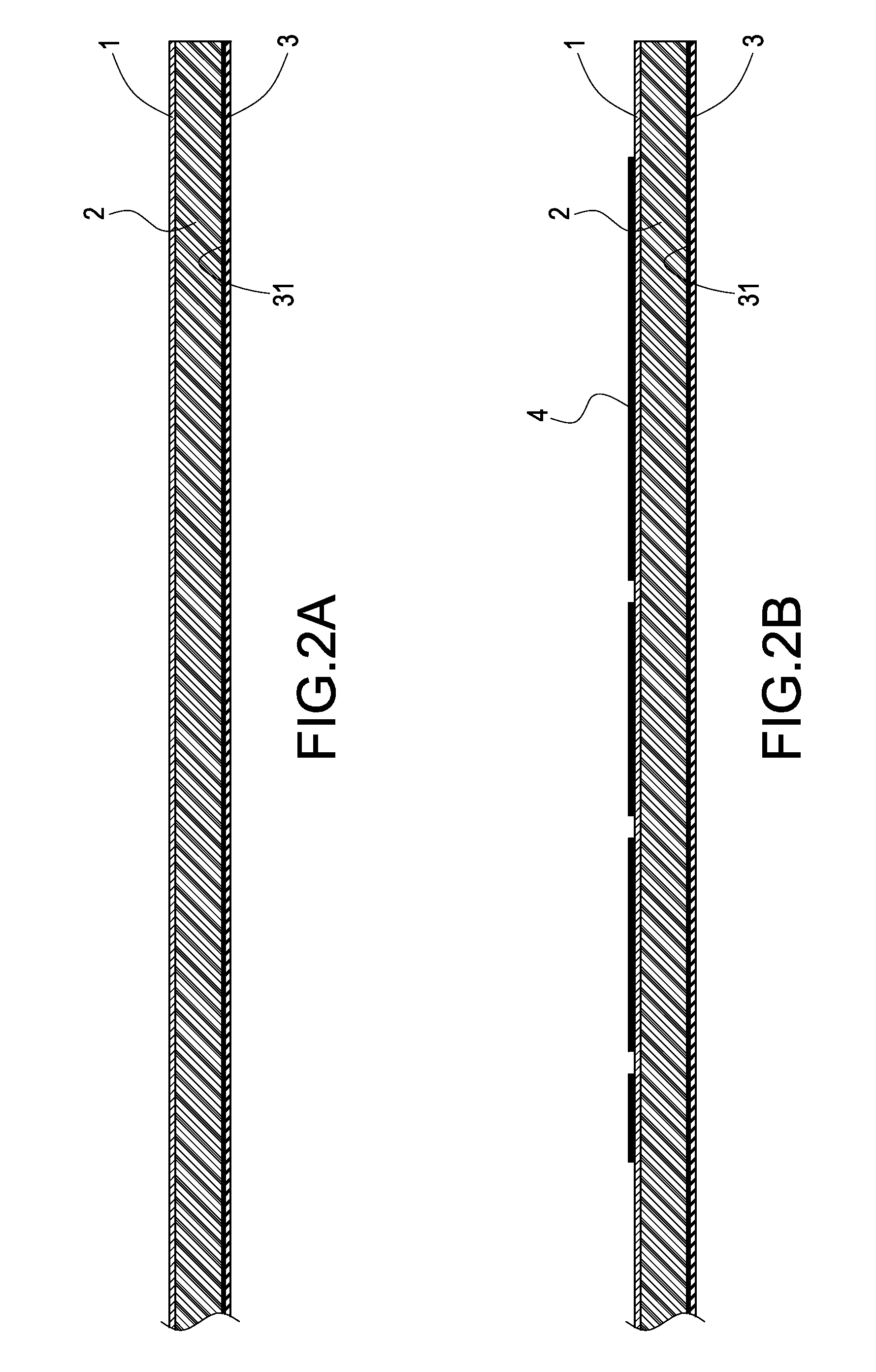
[0024]With reference to FIG. 1, it is a flow chart of the method for manufacturing the tag integrated circuit flexible board of the present invention and the associated electronic elements. As shown in this figure, the method for manufacturing a tag integrated circuit flexible board of the present invention comprises the steps as follows. Please also refer to FIG. 2A, first, in step 100, copper foil 1, an insulating heat-conductive material 2 and a base material 3 coated with an adhesive layer 31 are prepared. After being treated by a hot-pressing process, the copper foil 1, the insulating heat-conductive material 2 and the base material 3 are combined together to form a continuous band-like or sheet-like copper foil flexible board. In the drawings, the base material 3 is any one of a glue sheet or a thin metallic sheet. The thin metallic s...


PUM


Abstract

A structure of a tag integrated circuit flexible board includes a base material, one surface thereof having an adhesive layer; and a plurality of integrated circuit flexible boards that are arranged adjacent to one another and adhered on the adhesive layer of the base material. The integrated circuit flexible board includes an insulating heat-conductive material, and a conductive circuit layer provided on a surface of the insulating heat-conductive material and formed of a plurality of sections of circuits.

Description

[0001]This application is a divisional application of U.S. patent application Ser. No. 11 / 757,360, filed on Jun. 2, 2007.BACKGROUND OF THE INVENTION[0002]1. Field of the Invention[0003]The present invention relates to a flexible circuit board, and in particular to a structure of a tag flexible circuit board.[0004]2. Description of Prior Art[0005]When traditional light-emitting diodes are manufactured, a band-like or piece-like copper metallic plate is first pressed to form a plurality of lead frames that are connected with one another. A base is formed on each lead frame by means of a resin injection molding or hot press-forming process. The base has a cavity for allowing the lead frame to be exposed. Then, the lead frame in the cavity is subjected to a chip-fixing step and a wiring step. After finishing the chip-fixing and wiring steps, fluorescent glue and epoxy resin are dotted in the cavity to form a light-emitting diode.[0006]After the light-emitting diode is manufactured compl...

Claims


Application Information

Patent Timeline
Patent Type & Authority Applications(United States)
IPC IPC(8): H05K1/18
CPCH05K3/007H05K3/0097H05K3/064Y10T428/24917H05K2203/0152H05K2203/1545H05K3/341H01L2224/16H01L2924/181H01L2924/00012
Inventor WANG, PEI-CHOA
Owner PYROSWIFT HOLDING CO LIMITED
Learn More