Wafer processing method

a processing method and wafer technology, applied in heat-activated film/foil adhesives, solid-state devices, basic electric elements, etc., can solve the problems of supporting force, and possible damage to the wafer in grinding, so as to prevent possible damage to the bumps and the wafer, and reliably support

Active Publication Date: 2022-09-20
DISCO CORP
View PDF15 Cites 0 Cited by
  • Summary
  • Abstract
  • Description
  • Claims
  • Application Information

AI Technical Summary

Benefits of technology

[0008]It is therefore an object of the present invention to provide a wafer processing method which can ensure a sufficient supporting force for supporting the wafer to the substrate and can also prevent a degradation in quality of each device after separating the substrate from the wafer, without a reduction in productivity.
[0013]According to the present invention, the wafer can be supported to the substrate with a sufficient supporting force, so that possible damage to the wafer can be prevented in processing the back side of the wafer. Further, even when a plurality of bumps are formed on the front side of each device, the wafer can be reliably supported to the substrate in the condition where the bumps are embedded in the sheet softened by heating. Accordingly, stress applied to the wafer in the back processing step can be dispersed to thereby prevent possible damage to the bumps and the wafer.
[0014]Further, according to the processing method of the present invention, the wafer is united through the sheet to the substrate by thermocompression bonding. Accordingly, even in separating the sheet and the substrate from the front side of the wafer after performing the back processing step, there is no possibility that a liquid resin, adhesive, or wax may be left on the bumps. Accordingly, a degradation in quality of each device can be prevented.

Problems solved by technology

However, in the case of using the liquid resin to unite the wafer and the substrate, there is a problem such that a supporting force for supporting the wafer to the substrate is insufficient, so that the wafer cannot be stably held on a holding table in grinding the back side of the wafer, causing possible damage to the wafer in grinding.
However, also in this case, a supporting force for supporting the wafer to the substrate is insufficient as in the case of using the above-mentioned liquid resin, causing a similar problem.
In the case that a plurality of projection electrodes called bumps are formed on the front side of each device formed on the front side of the wafer, there arises a problem such that stress may be concentrated at the bumps in grinding the wafer unless the wafer is stably supported to the substrate, causing possible damage to the wafer.
Further, in separating the substrate from the front side of the wafer after finishing the grinding, there is a problem such that the liquid resin, adhesive of the double-sided adhesive tape, or wax may be left on the front side of the wafer due to adhesion, causing a degradation in quality of each device.
Accordingly, a step of removing the liquid resin, adhesive, or wax from the front side of the wafer must be added after separating the substrate from the wafer, causing a reduction in productivity.

Method used


Image

  • Wafer processing method
  • Wafer processing method
  • Wafer processing method

Examples


Embodiment Construction

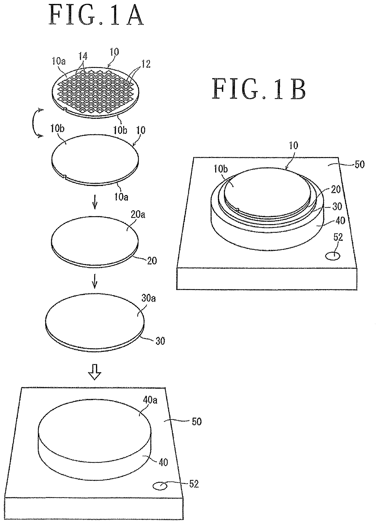
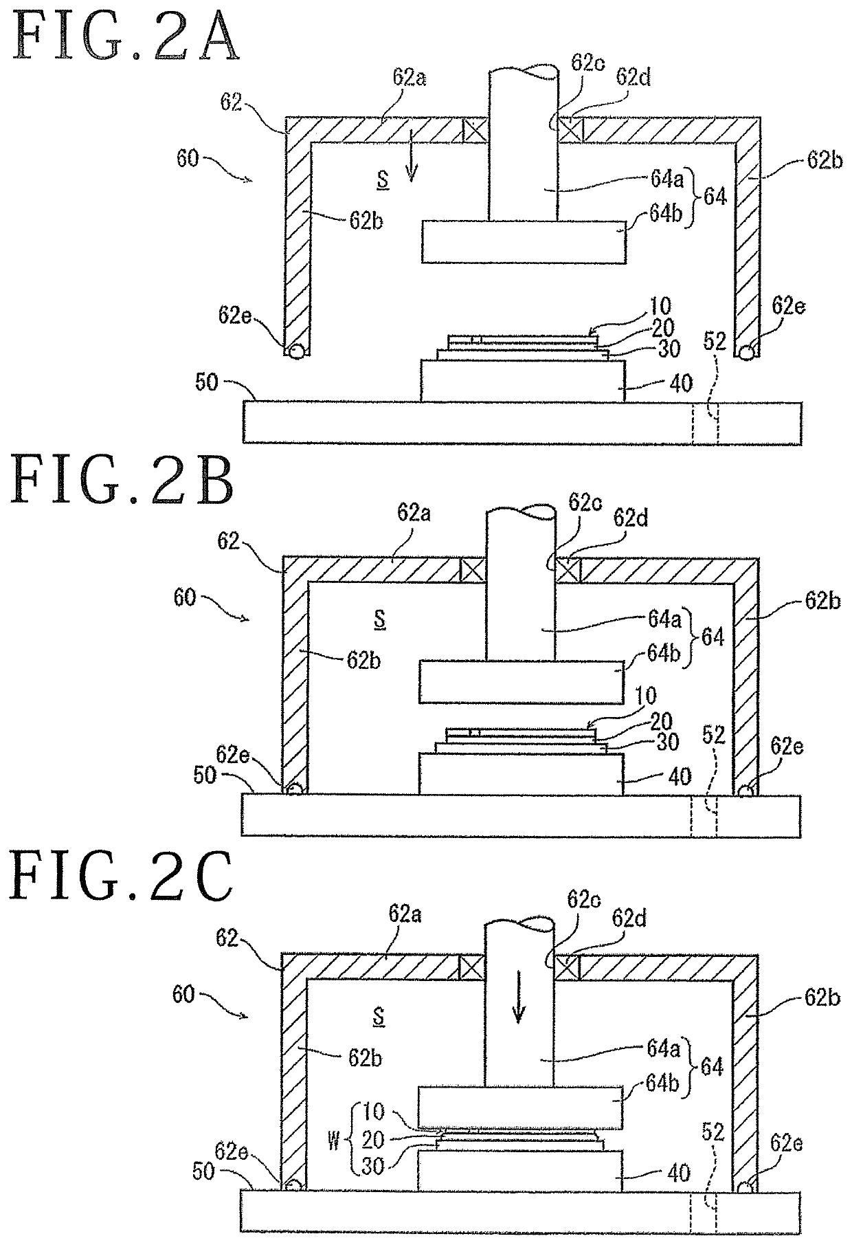
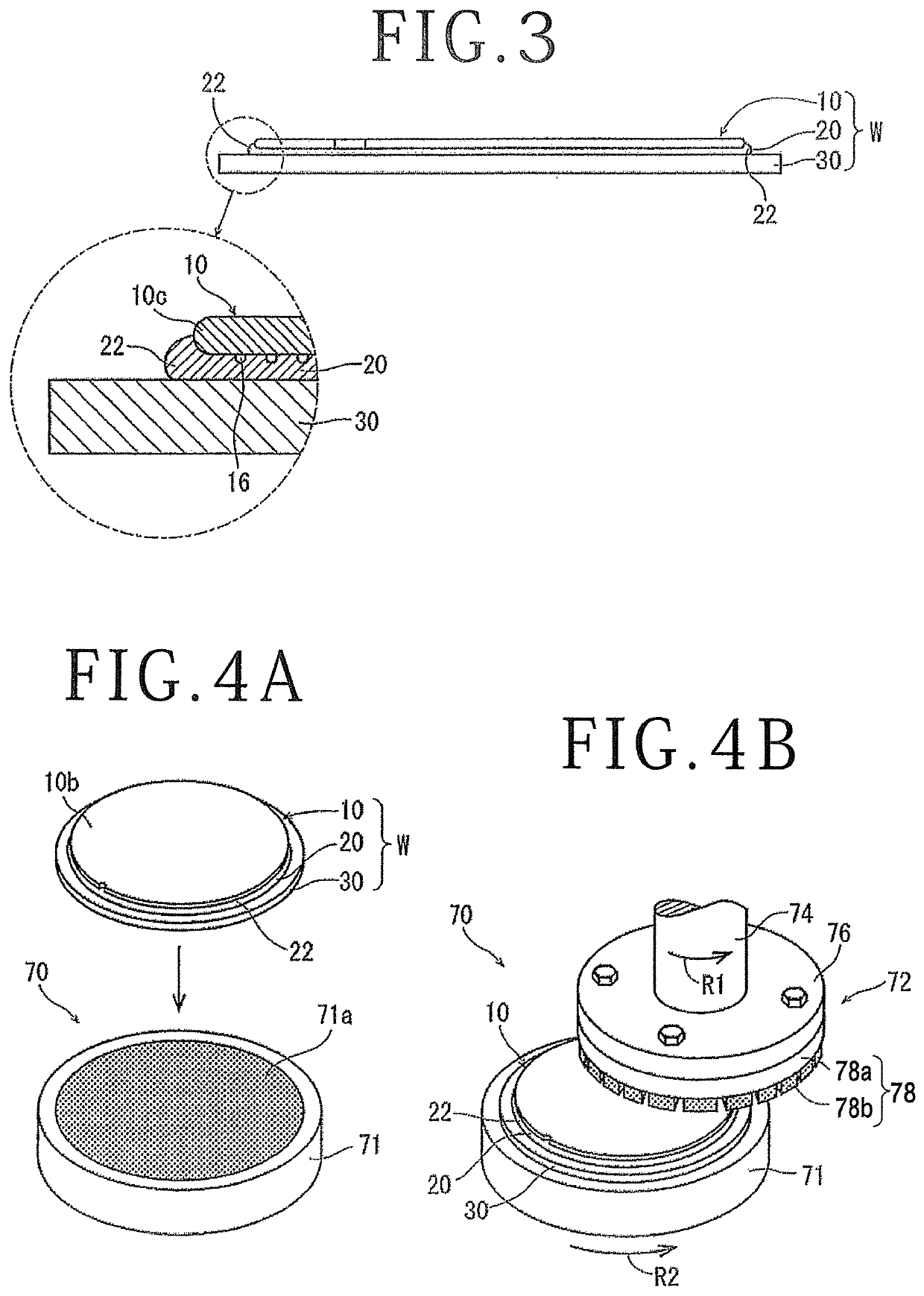
[0024]A preferred embodiment of the wafer processing method according to the present invention will now be described in detail with reference to the attached drawings. This preferred embodiment is a processing method for grinding the back side of a wafer. Prior to performing the wafer processing method according to this preferred embodiment, a circular wafer 10 as a workpiece is prepared as illustrated in FIG. 1A. As illustrated in FIG. 1A, the wafer 10 has a front side 10a and a back side 10b. A plurality of crossing division lines 14 are formed on the front side 10a of the wafer 10 to thereby define a plurality of separate regions where a plurality of devices 12 are individually formed. Further, a circular sheet 20 as a thermoplastic polymer sheet and a circular substrate 30 for supporting the wafer 10 are prepared. The sheet 20 has a front side 20a and a back side 20b. The substrate 30 has a front side 30a and a back side 30b.

(Wafer Providing Step)

[0025]After preparing the wafer...


PUM

PropertyMeasurementUnit
temperatureaaaaaaaaaa

Abstract

A wafer processing method includes a wafer providing step of placing a polyolefin or polyester sheet on an upper surface of a substrate for supporting a wafer and placing the wafer on an upper surface of the sheet in a condition where a back side of the wafer is exposed upward, a thermocompression bonding step of setting the wafer placed through the sheet on the substrate in an enclosed environment, next evacuating the enclosed environment, and next heating the sheet as applying a pressure to the wafer, thereby uniting the wafer through the sheet to the substrate by thermocompression bonding, a back processing step of processing the back side of the wafer supported through the sheet to the substrate, and a separating step of separating the wafer from the sheet bonded to the substrate.

Description

BACKGROUND OF THE INVENTIONField of the Invention[0001]The present invention relates to a wafer processing method for processing the back side of a wafer supported to a substrate.Description of the Related Art[0002]In processing a wafer having a plurality of devices such as integrated circuits (ICs) and large-scale integrations (LSIs) on the front side thereof, the plurality of devices being separated from each other by a plurality of crossing division lines formed on the front side of the wafer, the back side of the wafer is ground by using a grinding apparatus to thereby reduce the thickness of the wafer to a predetermined thickness. Thereafter, the wafer is divided along the division lines by using a dicing apparatus (dicing saw) to thereby obtain a plurality of individual device chips. These device chips are used in electrical equipment such as mobile phones and personal computers.[0003]In recent years, various kinds of device chips have been reduced in size and weight to meet t...

Claims


Application Information

Patent Timeline
Patent Type & Authority Patents(United States)
IPC IPC(8): H01L21/683C09J5/06C09J7/35H01L21/304H01L21/67H01L21/78H01L23/544
CPCH01L21/6836C09J5/06C09J7/35H01L21/304H01L21/67092H01L21/67132H01L21/78H01L23/544C09J2203/326C09J2301/502C09J2423/04C09J2423/10C09J2425/00C09J2467/00H01L2221/68327H01L2223/5446H01L21/02H01L21/6835H01L2221/6834H01L2221/68381H01L21/76H01L21/324H01L21/02016H01L21/682H01L21/67098
Inventor KIUCHI, HAYATOYAMAMOTO, KEISUKEKIMURA, TAICHIRO
Owner DISCO CORP
Why Eureka
Try Eureka