Method for fabricating thin film transistors

Inactive Publication Date: 2008-10-16
CHUNGHWA PICTURE TUBES LTD
View PDF4 Cites 1 Cited by
  • Summary
  • Abstract
  • Description
  • Claims
  • Application Information

AI Technical Summary

Benefits of technology

[0008]In order to solve the foregoing problems, one object of this invention is to apply the SLS or SSL technique to a portion of the substrate at first to perform the lateral growth and form a plurality of circuit areas, and then apply the LBELA technique to the whole area of the substrate, so as to widely promote the electric performance of the component, increase the component uniformity, and effectively fabricate the peripheral driving circuits on the panel edge, and furthermore to fabricate the System-On-Glass (SOG).
[0009]One object of this invention is to provide a method for fabricating thin film transistors, wherein a step of forming a thin oxidized layer on the substrate is added within the two laser irradiating steps, to eliminate the bias effect of the threshold voltage (Vth) caused by the second laser irradiation and furthermore to improve the interface stability between the polysilicon layer and the insulator.

Problems solved by technology

The polysilicon which has been irradiated by the flat-top excimer laser 10 has the advantage of uniform electric performance to be suitable for the pixel TFT However, the component quality is not good enough to be applied in the high-density integrated periphery circuits on the panel edge.
However, because the widths of the grains formed by the lateral growth technique are not uniform, the grain boundary may be forked or eliminated, as shown in the SEM image of FIG. 2, to cause the non-uniform electric performances and make the electric performances of the components perpendicular to the laser scan direction are poorer than the components parallel to the laser scan direction, to cause the troubling design for the circuit layout.
Although the SSL is applied effectively in this fabricating method, the last process of lateral growth still causes the poor uniformity of threshold voltage of the component, and the component differences between the perpendicular direction and the parallel direction still exist obviously.

Method used


Image

  • Method for fabricating thin film transistors
  • Method for fabricating thin film transistors
  • Method for fabricating thin film transistors

Examples


Embodiment Construction

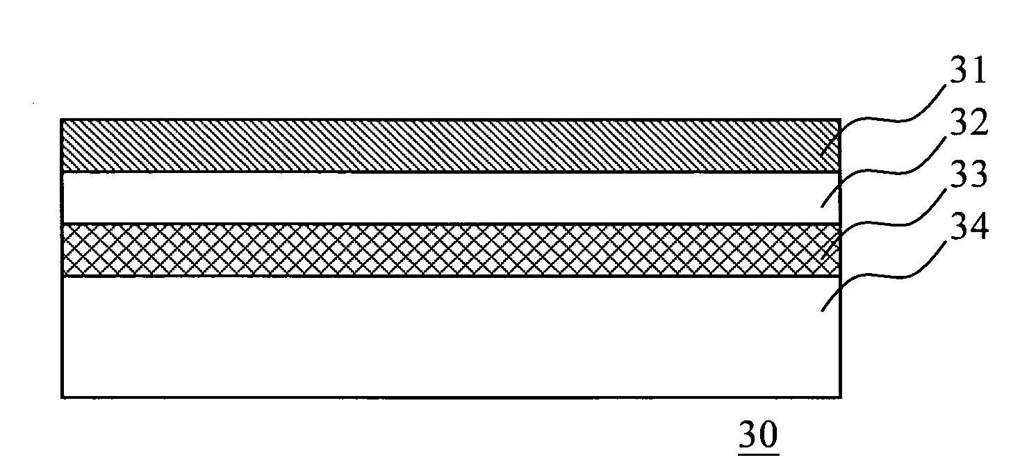
[0019]FIG. 3a and FIG. 3b are respectively a cross-sectional diagram and a vertical diagram illustrating an LTPS panel in accordance with an embodiment of the present invention. In the present embodiment, a substrate 30 is provided at first, wherein the bottom layer of the substrate 30 is a glass layer 34, and a silicon nitride (SiNx) film 33, a silicon oxide (SiOx) film 32 and an amorphous silicon (a-Si) film 31 are deposited on the glass layer 34 in order.

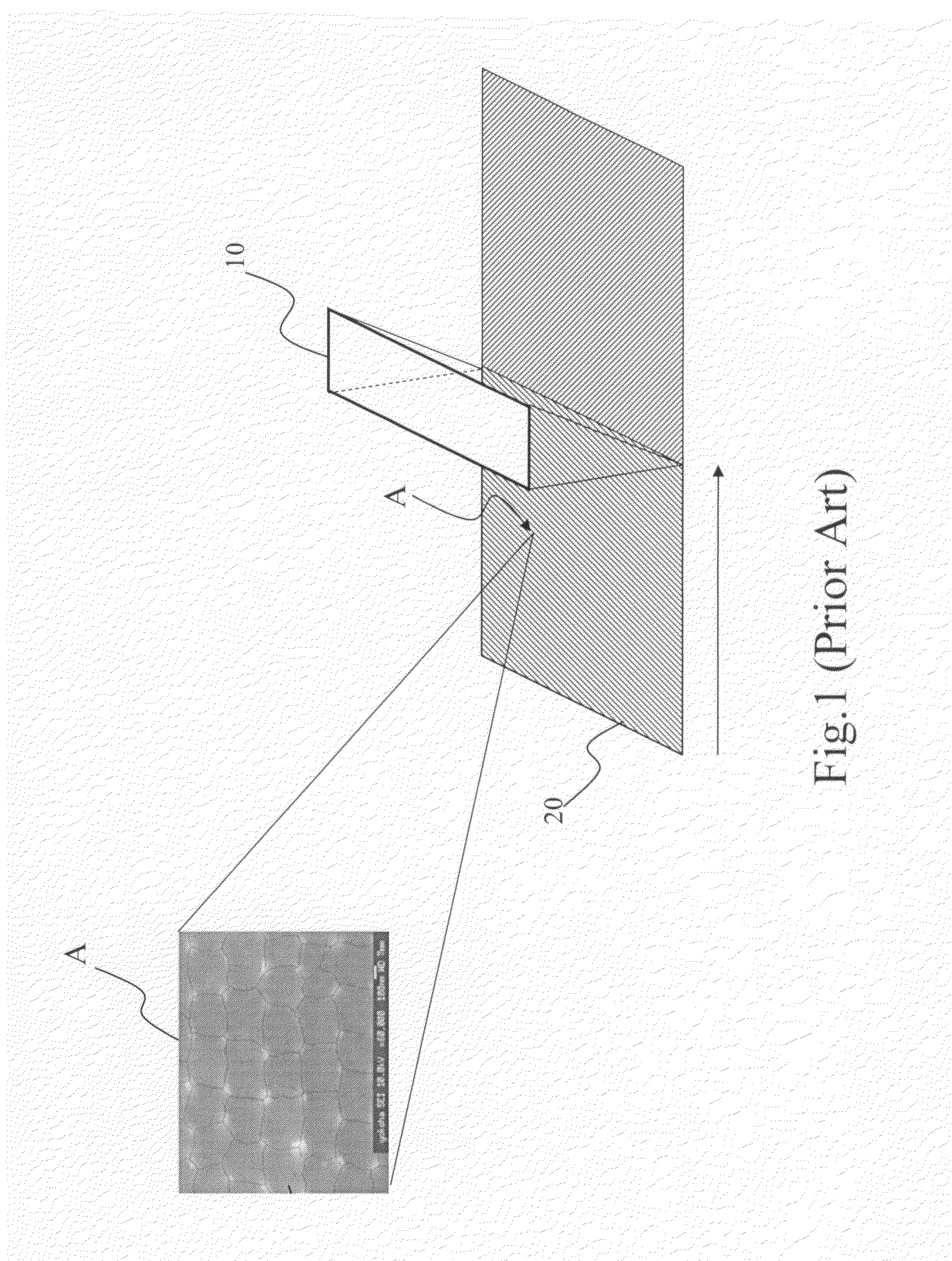
[0020]Next, please refer to FIG. 4 is a diagram illustrating the irradiating portion of the panel. In the process of crystal growing, the first laser irradiation is used to a portion 312 of the amorphous silicon film 31 to form a plurality of polysilicon regions, wherein the crystal growing technique is the laser annealing for lateral growth, such as the sequential lateral solidification (SLS), the solid state laser (SSL), or the thin beam directional crystallization (TDX), etc. In the following fabricating processes of LTPS, the...


PUM


Abstract

A method for fabricating thin film transistors is disclosed. An amorphous silicon film is formed on a substrated and selectively irradiated with a laser beam for lateral growth to form a plurality of polysilicon regions. The whole surface of the substrate is then oxidized and irradiated with exicer laser annealing.

Description

BACKGROUND OF THE INVENTION[0001]1. Field of the Invention[0002]The present invention relates to the method for fabricating a thin film transistors, and more especially, to the method for fabricating the TFT by using the low temperature polysilicon technology.[0003]2. Background of the Related Art[0004]The fabrication technologies of the thin film transistor liquid crystal display (TFT LCD) include the polysilicon technique and the amorphous silicon technique. Now, the amorphous silicon technique is mature and widely used. The low temperature polysilicon technique (LTPS) is a newly fabricating process for the TFT LCD. The carrier mobility of the LTPS is two hundred times than the mobility of the amorphous silicon, and the difference between the traditional amorphous silicon display and the LTPS display is that the LTPS display has the advantages of high performance, high brightness and high resolution. If the LTPS display is applied to the notebook, the power of the notebook will be...

Claims


Application Information

Patent Timeline
IPC IPC(8): H01L21/84
CPCH01L21/02422H01L21/02532H01L27/1285H01L21/02686H01L21/02675
Inventor SHIH, CHIH-JENYEH, WEN-CHUNHO, MIN-CHEYANG, WEN-CHI
Owner CHUNGHWA PICTURE TUBES LTD
Why Eureka
Try Eureka