Dynamic temperature backside gas control for improved within-substrate process uniformity

a backside gas and dynamic temperature technology, applied in individual semiconductor device testing, semiconductor/solid-state device testing/measurement, instruments, etc., can solve the problems of increasing reducing the size of features, and increasing the complexity of devices formed on semiconductor substrates. achieve the effect of improving process uniformity in semiconductor manufacturing

Active Publication Date: 2008-09-18
TOKYO ELECTRON LTD +1
View PDF6 Cites 16 Cited by
  • Summary
  • Abstract
  • Description
  • Claims
  • Application Information

AI Technical Summary

Benefits of technology

[0011]A general objective of the present invention is to improve process uniformity in semiconductor manufacturing across the surfaces of substrates during processing.

Problems solved by technology

In semiconductor manufacturing, the complexity of devices formed on semiconductor substrates continues to increase at a rapid pace, while the size of features, such as transistor gates, continues to decrease well below the 93 nanometer (nm) technology node.
However, these systems facilitate only static distributions of the heat transfer gas.

Method used


Image

  • Dynamic temperature backside gas control for improved within-substrate process uniformity
  • Dynamic temperature backside gas control for improved within-substrate process uniformity
  • Dynamic temperature backside gas control for improved within-substrate process uniformity

Examples


Embodiment Construction

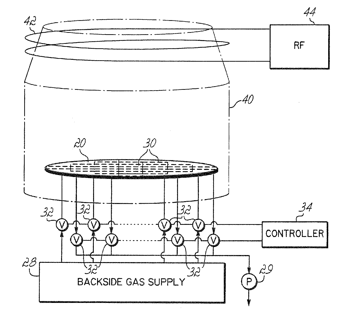
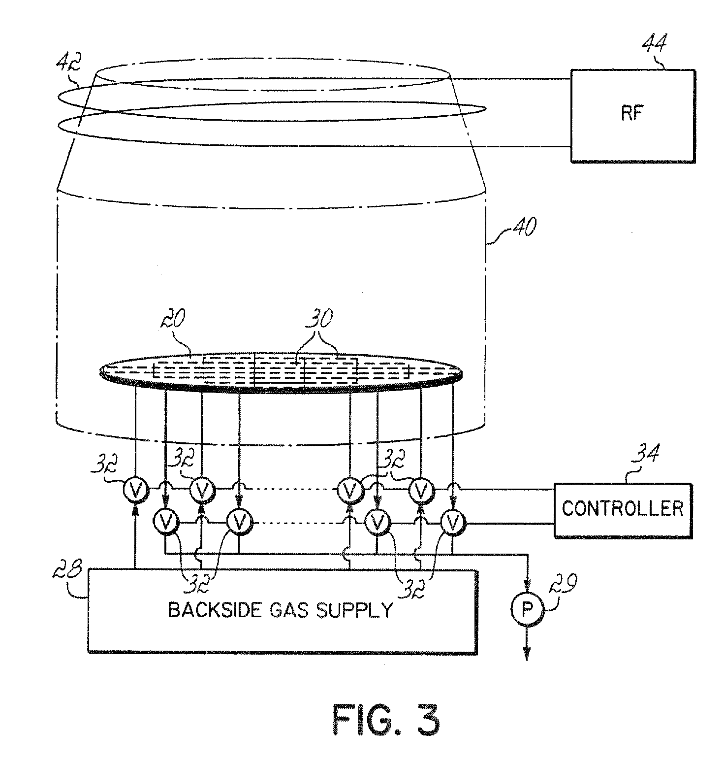
[0032]In the following description, for purposes of explanation and not limitation, specific details are set forth, such as a particular geometry of the substrate processing system and descriptions of various processes. However, it should be understood that the invention may be practiced in other embodiments that depart from these specific details.

[0033]The substrate processing system can comprise a plasma processing system configured to treat a substrate with plasma. Alternatively, the substrate processing system can comprise a non-plasma processing system configured to treat a substrate. The substrate processing system may comprise an etching system that utilizes plasma to facilitate a dry etching process during semiconductor manufacturing. Examples of an etching system are provided in U.S. Pat. No. 6,492,612 and PCT Publication WO 02 / 086957; each of which are hereby expressly incorporated herein by reference. Nonetheless, the invention can be used for improving uniformity in depo...


PUM

PropertyMeasurementUnit
Temperatureaaaaaaaaaa
Pressureaaaaaaaaaa
Diameteraaaaaaaaaa

Abstract

A method and apparatus are provided to control the radial or non-radial temperature distribution across a substrate during processing to compensate for non-uniform effects, including radial and angular non-uniformities arising from system variations, or process variations, or both. The temperature is controlled, preferably dynamically, by flowing backside gas differently across different areas on a wafer supporting chuck to vary heat conduction across the wafer. Backside gas flow, of helium, for example, is dynamically varied across the chuck to control the uniformity of processing of the wafer. Ports in the support are grouped, and gas to or from the groups is separately controlled by different valves responsive to a controller that controls gas pressure in each of the areas to spatially and preferably dynamically control wafer temperature to compensate for system and process non-uniformities.

Description

[0001]This application is related to commonly assigned U.S. patent application Ser. No. ______ entitled “Dynamic Control Of Process Chemistry For Improved Within-Substrate Process Uniformity” by the inventors hereof, filed on even date herewith, and commonly assigned U.S. patent application Ser. No. ______ entitled “Method For Flexing A Substrate During Processing”, filed on even date herewith by Merritt Funk; and hereby expressly incorporated by reference herein.FIELD OF THE INVENTION[0002]This invention relates to the control of process uniformity across a substrate, including, for example, process uniformity during an etching process performed on a substrate. The invention particularly relates to the control of process uniformity across a substrate by control of the substrate temperature.BACKGROUND OF THE INVENTION[0003]In semiconductor manufacturing, the complexity of devices formed on semiconductor substrates continues to increase at a rapid pace, while the size of features, su...

Claims


Application Information

Patent Timeline
IPC IPC(8): H01L21/306H01L21/66
CPCH01L22/20
Inventor SUNDARARAJAN, RADHACHEN, LEEFUNK, MERRITT
Owner TOKYO ELECTRON LTD
Why Eureka
Try Eureka