
Circuit board surface structure

a surface structure and circuit board technology, applied in the direction of resist details, non-metallic protective coating application, semiconductor/solid-state device details, etc., can solve the problem of reducing the contact area between the solder structure, difficult to form a solder material, and failing to meet the requirement for fine pitch of the electrically connecting pad in advanced electronic products, etc., to achieve the effect of sufficient bonding strength

Inactive Publication Date: 2008-09-11
UNIMICRON TECH CORP
View PDF5 Cites 25 Cited by
  • Summary
  • Abstract
  • Description
  • Claims
  • Application Information

AI Technical Summary

Benefits of technology

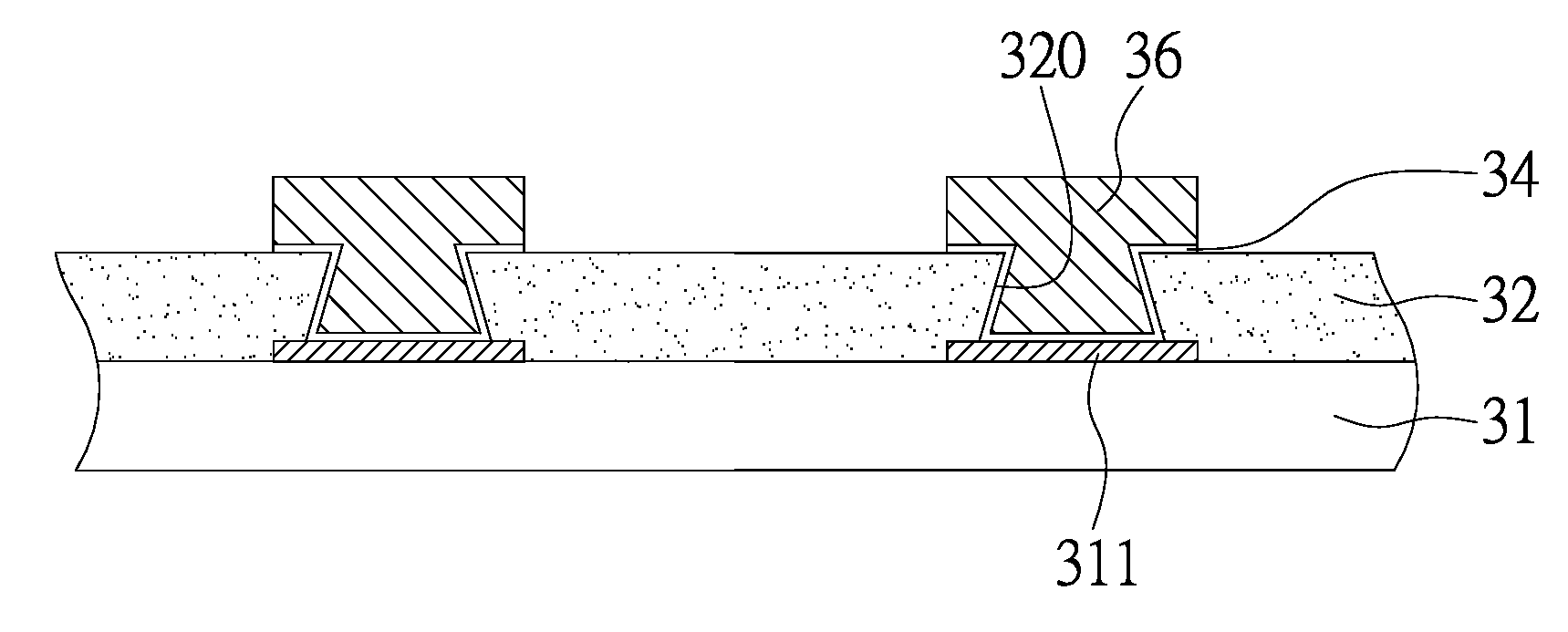
[0010]In light of the foregoing drawbacks of the prior art, a primary objective of the present invention is to provide a circuit board surface structure with enhanced bonding strength between the conductive elements and the circuit board.
[0015]In summary, the circuit board surface structure of the present invention, mainly involves forming a solder mask layer on the circuit board having electrically connecting pads, then through exposure and development process with quantitative control of heat and light, openings tapered upward are formed in the insulating protective layer, allowing the electrically connecting pads 31 to have a larger exposed contact area, so as to increase the contact area between the conductive elements and the electrically connecting pads, and reinforce bonding between the conductive elements in the openings of the insulating protective layer and the electrically connecting pads. Moreover, the present invention provides sufficient bonding strength for the conductive elements formed on the fine pitch electrically connecting pads, thereby eliminating a drawback of the prior art, that is, difficulty in attaching a solder material to the surface of electrically connecting pads.

Problems solved by technology

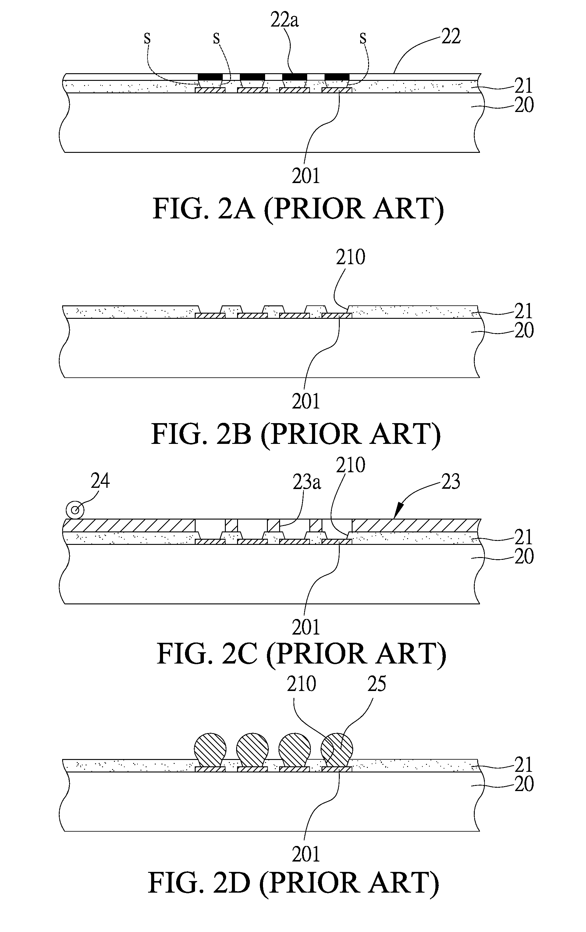
As a gap between the circuits is reduced, the opening on the solder mask layer above the electrically connecting pads must be miniaturized further, and this may reduce the contact area between the solder structure and electrically connecting pad, such that it is more difficult to form a solder material on the electrically connecting pad, thereby failing to satisfy the requirement for fine pitch of the electrically connecting pads in advanced electronic products.

Method used


Image

  • Circuit board surface structure
  • Circuit board surface structure
  • Circuit board surface structure

Examples


Embodiment Construction

[0020]The present invention is described in the following with specific embodiments, so that one skilled in the pertinent art can easily understand other advantages and effects of the present invention from the disclosure of the present invention.

[0021]FIGS. 3A-3I are cross-sectional views showing how to fabricate a circuit board surface structure of the present invention.

[0022]Referring to FIG. 3A, a circuit board 31 resulted from a front end patterning process is provided. A plurality of electrically connecting pads 311, and optionally a plurality of conductive circuits (not shown), are formed on at least one surface of the circuit board 31. There are numerous complicated processes of forming conductive circuits and electrically connecting pads on a circuit board. The processes are widely known by those skilled in the art, but are irrelevant to essential technical features of the present invention. Therefore, the processes are not described herein.

[0023]Referring to FIG. 3B, an in...


PUM


Abstract

A circuit board surface structure includes a circuit board having at least one surface provided with a plurality of electrically connecting pads, an insulating protective layer characterized by photosensitivity and solder resisting and formed on the circuit board, and a plurality of openings formed in the insulating protective layer to expose the electrical connecting pads on the circuit board and tapered upward; and a conductive element formed in the opening, so as to increase the contact area and reinforce bonding between the electrically connecting pads and the conductive element.

Description

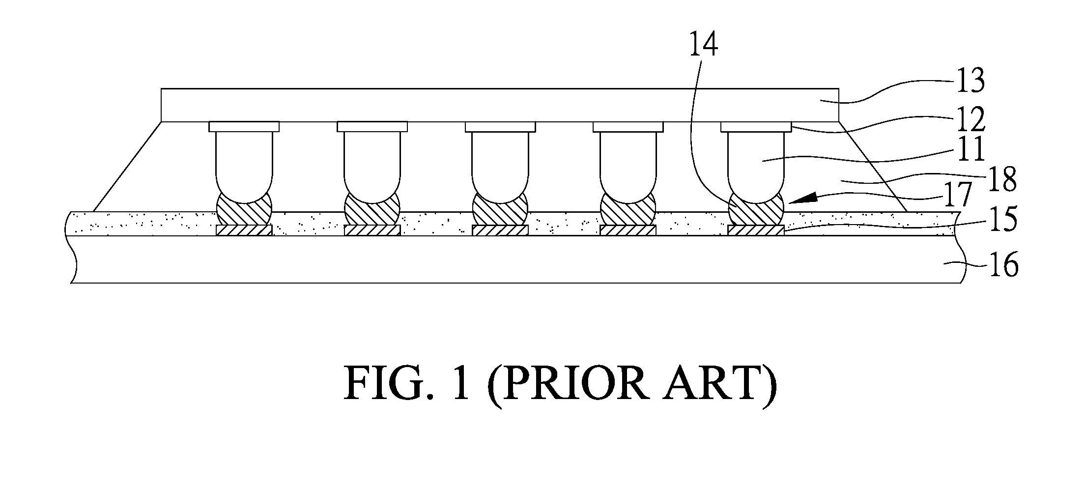
BACKGROUND OF THE INVENTION[0001]1. Field of the Invention[0002]The present invention relates to circuit board surface structures, and more particularly, to a circuit board surface structure comprising a circuit board with electrically connecting pads having conductive elements formed thereon for external electrical connection.[0003]2. Description of the Prior Art[0004]According to flip chip technology nowadays, a semiconductor chip is electrically connected to a circuit board, in which electrode pads are provided on the active surface of the integrated circuit-equipped (IC-equipped) semiconductor chip, and the circuit board is provided with electrically connecting pads corresponding to the electrode pads. A solder structure or other conductive adhesive material is formed between the electrode pad of the semiconductor chip and the electrically connecting pad of the circuit board for providing electrical connection and mechanical coupling between the semiconductor chip and the circui...

Claims


Application Information

Patent Timeline
Patent Type & Authority Applications(United States)
IPC IPC(8): H05K1/09H05K1/00H05K1/11
CPCH01L23/49811H01L2224/16H01L2924/01079H05K3/0023H05K2203/0594H05K3/28H05K3/3452H05K3/3473H05K2203/054H05K3/243H01L2224/05022H01L2224/05001H01L2224/05572H01L2224/05111H01L2224/05147H01L2224/05155H01L2224/05166H01L2224/05171H01L2224/05611H01L2224/05647H01L2224/05655H01L2224/05666H01L2224/05671H01L2224/05601H01L2224/05605H01L2224/05609H01L2224/05613H01L2224/05616H01L2224/05618H01L2224/0562H01L2224/05623H01L2224/05639H01L2224/05644H01L2224/0567H01L24/13H01L2924/01024H01L2924/01082H01L2924/013H01L2924/00014
Inventor HU, WEN-HUNG
Owner UNIMICRON TECH CORP
Learn More