Optical semiconductor device and fabrication process thereof

a technology of optical semiconductor and fabrication process, applied in the direction of semiconductor lasers, instruments, optical elements, etc., can solve the problems of optical modulator, increased parasitic capacitance, and difficulty in the operation of laser diodes at high speed

Active Publication Date: 2008-07-24
SUMITOMO ELECTRIC DEVICE INNOVATIONS
View PDF4 Cites 17 Cited by
  • Summary
  • Abstract
  • Description
  • Claims
  • Application Information

AI Technical Summary

Benefits of technology

[0036]said step of depositing said semi-insulating buried semiconductor layer being further conducted such that, in said second region, said semi-insulating buried semiconductor layer fills said gap between said plurality of dummy mesa patterns with a thickness that does not become lower than a height of said plurality of dummy mesa patterns.

Problems solved by technology

Similar problem arises also in the optical modulator that includes an optical absorption layer.
On the other hand, with the construction of the Patent Reference 1, there arises a problem, in view of the fact that the regions at the lateral sides of the mesa structure constituting the laser diode are buried with the p / n carrier blocking layers, in that there is caused an increase of parasitic capacitance.
It should be noted that such increase of the parasitic capacitance invites difficulty for the laser diode to operate at high speed.
When there is caused a minute deviation from these specific directions, there arises a problem that the buried layers form eaves defined by the (111)A surface on the mesa stripe by growing in the direction to face each other.
Further, with such a laser diode, there is a tendency that the yield of production is degraded.
Because of the formation of such a sloped part 26E adjacent to the flat part 26D, there arises a problem in that it becomes difficult to inject the optical beam exited from the mesa stripe 22M into the optical waveguide such as an optical fiber in the event an optical window is formed in the exit direction of the mesa stripe 22M.
While formation of such a sloped part 26D can be resolved when the growth of the InP buried layer 26 is continued over a prolonged time, such an approach wastes the source material and tends to invite various problems such as degradation of production throughput, frequent equipment maintenance, and the like.
Thus, such an approach is deemed not realistic to mass production of semiconductor devices.

Method used


Image

  • Optical semiconductor device and fabrication process thereof
  • Optical semiconductor device and fabrication process thereof
  • Optical semiconductor device and fabrication process thereof

Examples


first embodiment

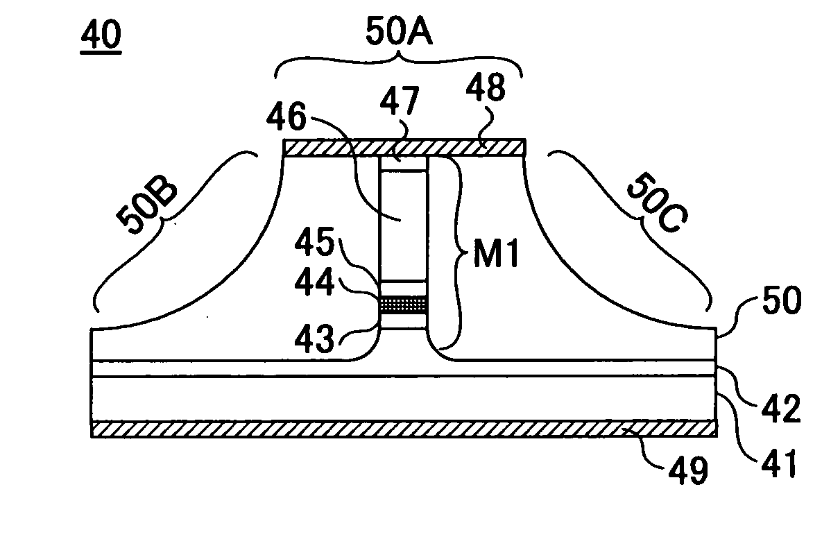
[0043]FIGS. 3A-3D show the construction of an optical semiconductor device 40 according to a first embodiment of the present invention.

[0044]Referring to FIGS. 3A-3D, the optical semiconductor device 40 is a semiconductor optical amplifier (SOA) and is constructed on an n-type InP substrate 40 having a (100) principal surface. Here, it should be noted that FIG. 3A shows the laser diode 40 in a plan view, FIG. 3B shows the laser diode 40 in a cross-sectional view taken along a line A-A′ of FIG. 3A, FIG. 3C shows the laser diode 40 in a cross-sectional view taken aling a line B-B′ of FIG. 3A, while FIG. 3D is a longitudinal cross-sectional view taken along a line C-C′ of FIG. 3A.

[0045]Referring to the cross-sectional view of FIG. 3B at first, there is formed an InP lower cladding layer 42 doped to n-type with the carrier density of 1.0×1018 cm−3 on the n-type InP substrate 41 epitaxially with a thickness of 0.3 μm, for example, and a lower SCH (separate confinement heterostructure) la...

second embodiment

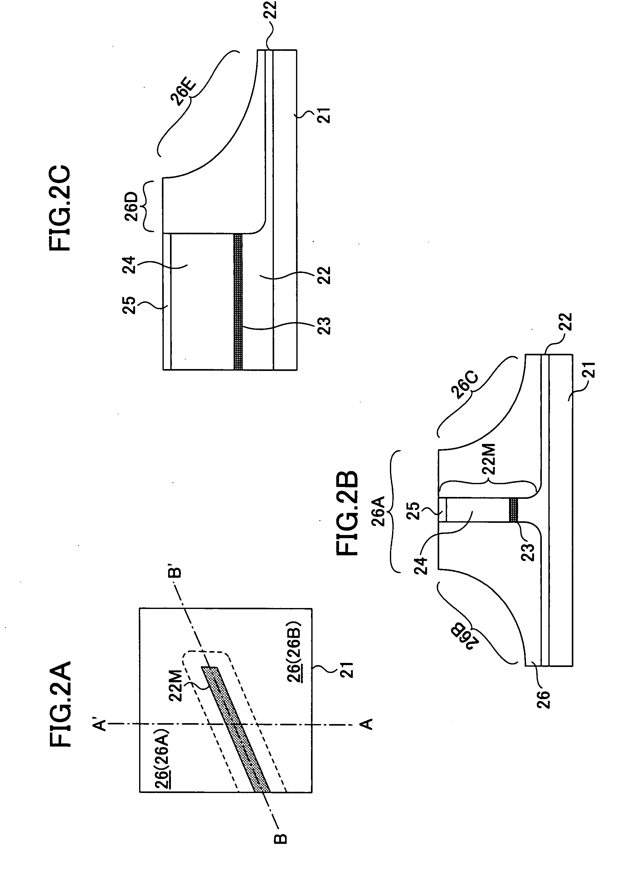
[0070]FIGS. 5A-5D show the construction of an optical semiconductor device 60 according to a second embodiment of the present invention. In the drawings, those parts explained before are designated by the same reference numerals and the description thereof will be omitted.

[0071]Referring to the plan view diagram of FIG. 5A, each of the mesa stripes M1-M3 is formed on the InP substrate 41 with the direction offset from the direction toward the [0-11] direction by the angle of 10° with the optical semiconductor device 60 of the present embodiment.

[0072]Further, with the present embodiment, 1,2 dichloroethylene is added at the time of deposition of the InP buried layer 50 in place of the methyl chloride with a flow rate of 50 sccm.

[0073]In the present embodiment, too, the mesa stripes M1-M3 have a width of 2 μm and a height of 3 μm and are formed with a separation of 10 μm or more but not exceeding 50 μm, such as 30 μm, when viewed from the extending direction of the mesa stripe M1. Th...


PUM


Abstract

An optical semiconductor, includes a semiconductor substrate having a (100) principal surface, a waveguide mesa stripe formed on a first region of the semiconductor substrate, the waveguide mesa stripe guiding a light therethrough; a plurality of dummy mesa patterns formed on the semiconductor substrate in a second region at a forward side of the first region, and a semi-insulating buried semiconductor layer formed on the semiconductor substrate so as to cover the first and second regions continuously, the semi-insulating buried semiconductor layer filling a right side and a left side of the waveguide mesa stripe in the first region and a gap between the plurality of dummy mesa patterns in the second region.

Description

CROSS-REFERENCE TO RELATED APPLICATION[0001]The present application is based on Japanese priority application No. 2007-010235 filed on Jan. 19, 2007, the entire contents of which are hereby incorporated by reference.BACKGROUND OF THE INVENTION[0002]The present invention generally relates to semiconductor devices and more particularly to an optical semiconductor device including semiconductor optical amplifier, laser diode, optical modulator, and the like.[0003]In optical communication networks, there is a demand for the optical semiconductor device used therein such as a semiconductor optical amplifier, laser diode, optical modulator, and the like, in that the optical semiconductor device operates stably and at high speed. In the optical semiconductor device that includes therein an optical amplification part such as semiconductor optical amplifier or laser diode, in particular, reflection caused at the exit end surface serving for optical window tends to invite adversary effect on ...

Claims


Application Information

Patent Timeline
Patent Type & Authority Applications(United States)
IPC IPC(8): H01S5/227H01L33/00
CPCB82Y20/00H01S5/026H01S5/1085H01S5/16H01S5/2201H01S5/2224H01S2304/04H01S5/2275H01S5/3211H01S5/34306H01S5/34373H01S5/50H01S5/227
Inventor UETAKE, AYAHITOTAKEUCHI, TATSUYA
Owner SUMITOMO ELECTRIC DEVICE INNOVATIONS
Why Eureka
Try Eureka