Low-cost strained soi substrate for high-performance CMOS technology

a technology of strained soi and cmos, which is applied in the direction of semiconductor devices, electrical equipment, transistors, etc., can solve the problems of complex and expensive prior art methods of fabricating strained soi substrates, material and process integration challenges, and the inability to build transistors on top of sige layers, etc., to achieve high carrier mobility, avoid epitaxial growth and subsequent wafer bonding processing steps, cost-effect and simple

Inactive Publication Date: 2008-07-17
GLOBALFOUNDRIES INC
View PDF9 Cites 34 Cited by
  • Summary
  • Abstract
  • Description
  • Claims
  • Application Information

AI Technical Summary

Benefits of technology

[0007]The present invention provides a cost-effect and simple method of fabricating a SSOI structure which avoids epitaxial growth and subsequent wafer bonding processing steps. In accordance with the present invention, a strain-...

Problems solved by technology

However, the presence of the SiGe layer causes material and process integration challenges.
The need to thin the active Si and SiGe layers for high-performance complementary metal oxide semiconductor (CMOS) technology makes the appro...

Method used


Image

  • Low-cost strained soi substrate for high-performance CMOS technology
  • Low-cost strained soi substrate for high-performance CMOS technology
  • Low-cost strained soi substrate for high-performance CMOS technology

Examples


Embodiment Construction

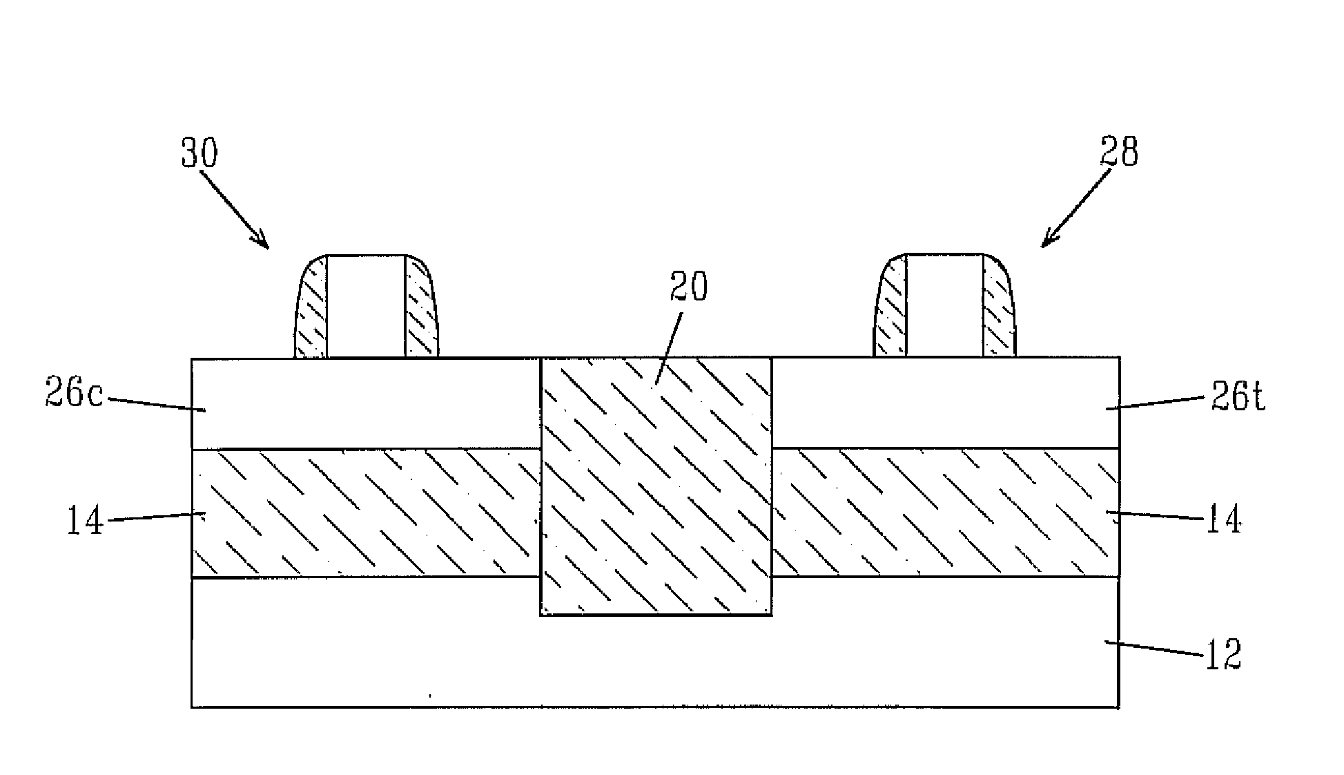
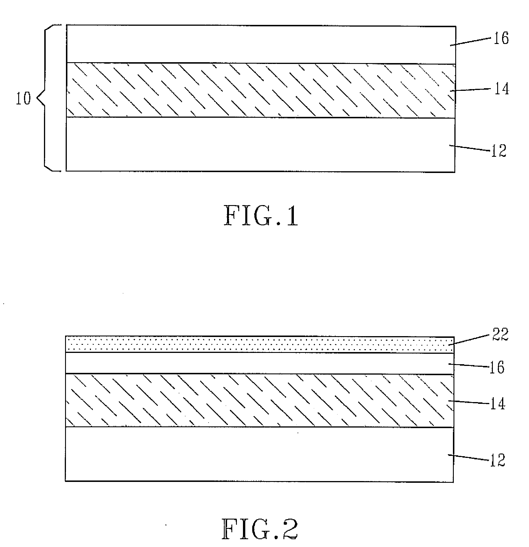
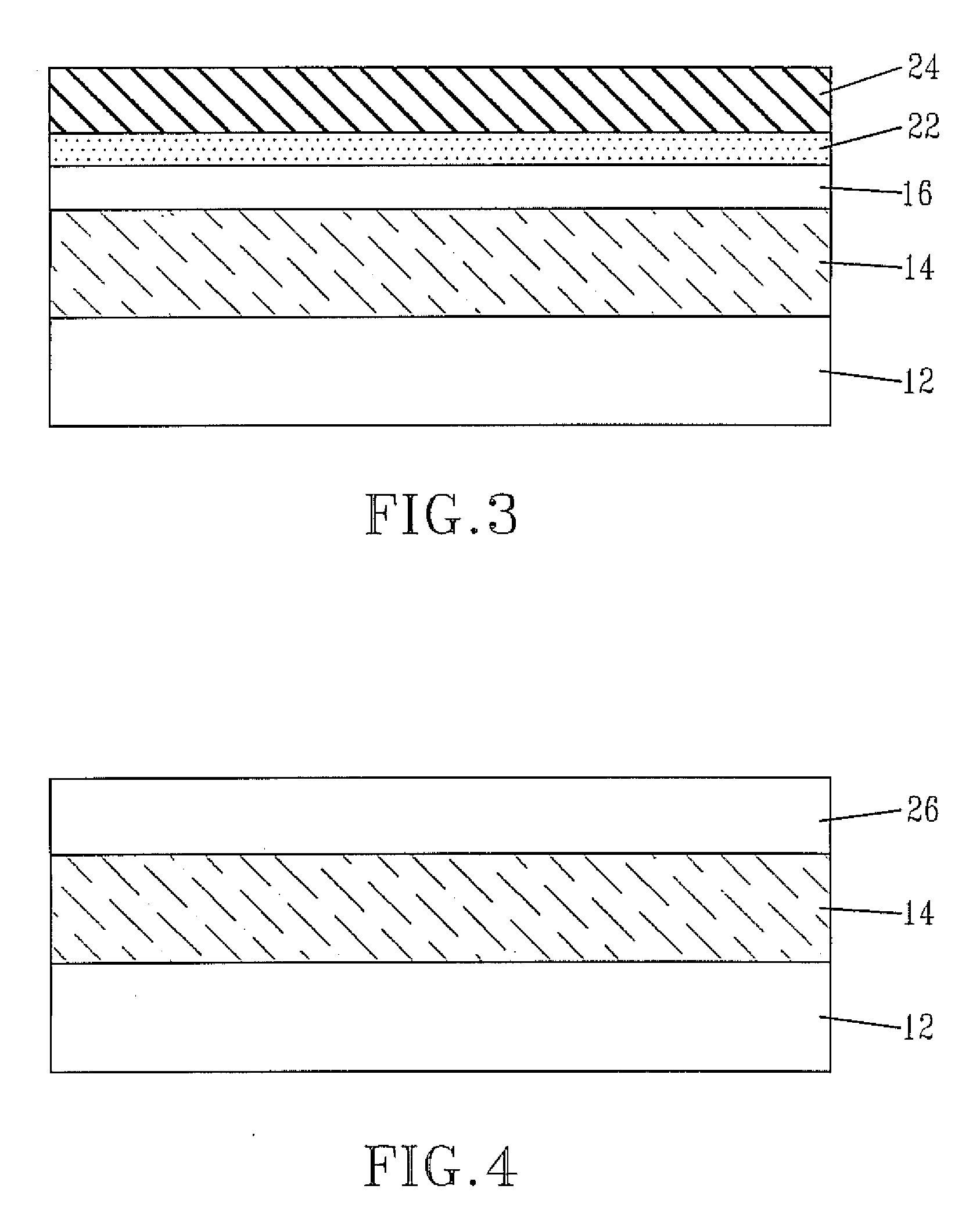
[0021]The present invention, which provides a method of fabricating a strained semiconductor-on-insulator (SSOI) substrate as well a method of fabricating devices atop the SSOI substrate, will now be described in greater detail by referring to the following discussion and drawings that accompany the present application. It is noted that the drawings of the present application are provided for illustrative purposes and, as such, the drawings are not drawn to scale.

[0022]In the following description, numerous specific details are set forth, such as particular structures, components, materials, dimensions, processing steps and techniques, in order to provide a thorough understanding of the present invention. However, it will be appreciated by one of ordinary skill in the art that the invention may be practiced with viable alternative process options without these specific details. In other instances, well-known structures or processing steps have not been described in detail in order t...


PUM


Abstract

A cost-effective and simple method of fabricating strained semiconductor-on-insulator (SSOI) structures which avoids epitaxial growth and subsequent wafer bonding processing steps is provided. In accordance with the present invention, a strain-memorization technique is used to create strained semiconductor regions on a SOI substrate. The transistors formed on the strained semiconductor regions have higher carrier mobility because the Si regions have been strained. The inventive method includes (i) ion implantation to create a thin amorphization layer, (ii) deposition of a high stress film on the amorphization layer, (iii) a thermal anneal to recrystallize the amorphization layer, and (iv) removal of the stress film. Because the SOI substrate was under stress during the recrystallization process, the final semiconductor layer will be under stress as well. The amount of stress and the polaity (tensile or compressive) of the stress can be controlled by the type and thickness of the stress films.

Description

FIELD OF THE INVENTION[0001]The present invention relates to semiconductor fabrication and more particularly to a method of fabricating a strained semiconductor-on-insulator (SSOI) substrate. The present invention also provides a method of fabricating devices atop the SSOI substrate.BACKGROUND OF THE INVENTION[0002]In the semiconductor industry, it is well known that device performance can be increased by introducing strain into a semiconductor channel of a metal oxide semiconductor field effect transistor (MOSFET). A strained semiconductor channel can be produced, for example, by depositing Si epitaxially on a relaxed SiGe material. The strain is created from the difference in lattice spacing between Si and SiGe.[0003]Conventional strained Si typically uses a relatively thick (on the order of about 500 nm or greater) layer of SiGe to exert a strain on a top layer of relatively thin (on the order of about 20 nm or less) Si. The larger Ge atoms stretch or strain the top lattice of Si...

Claims


Application Information

Patent Timeline
IPC IPC(8): H01L21/20
CPCH01L21/02658H01L21/02667H01L21/26506H01L29/7843H01L21/823878H01L21/84H01L29/78H01L21/823807
Inventor IEONG, MEIKEILA TULIPE, DOUGLAS C.SHI, LEATHENTOPOL, ANNA W.VICHICONTI, JAMESYOUNG, ALBERT M.
Owner GLOBALFOUNDRIES INC
Why Eureka
Try Eureka