
High-current traces on plated molded interconnect device

a technology of high-current traces and interconnect devices, which is applied in the field of high-current traces on plated, can solve the problems of limiting the width of the trace, the cost of the plating process usually limiting the depth of the trace, and the cost of the plating process

Inactive Publication Date: 2008-07-17
MOLEX INC
View PDF0 Cites 24 Cited by
  • Summary
  • Abstract
  • Description
  • Claims
  • Application Information

AI Technical Summary

Benefits of technology

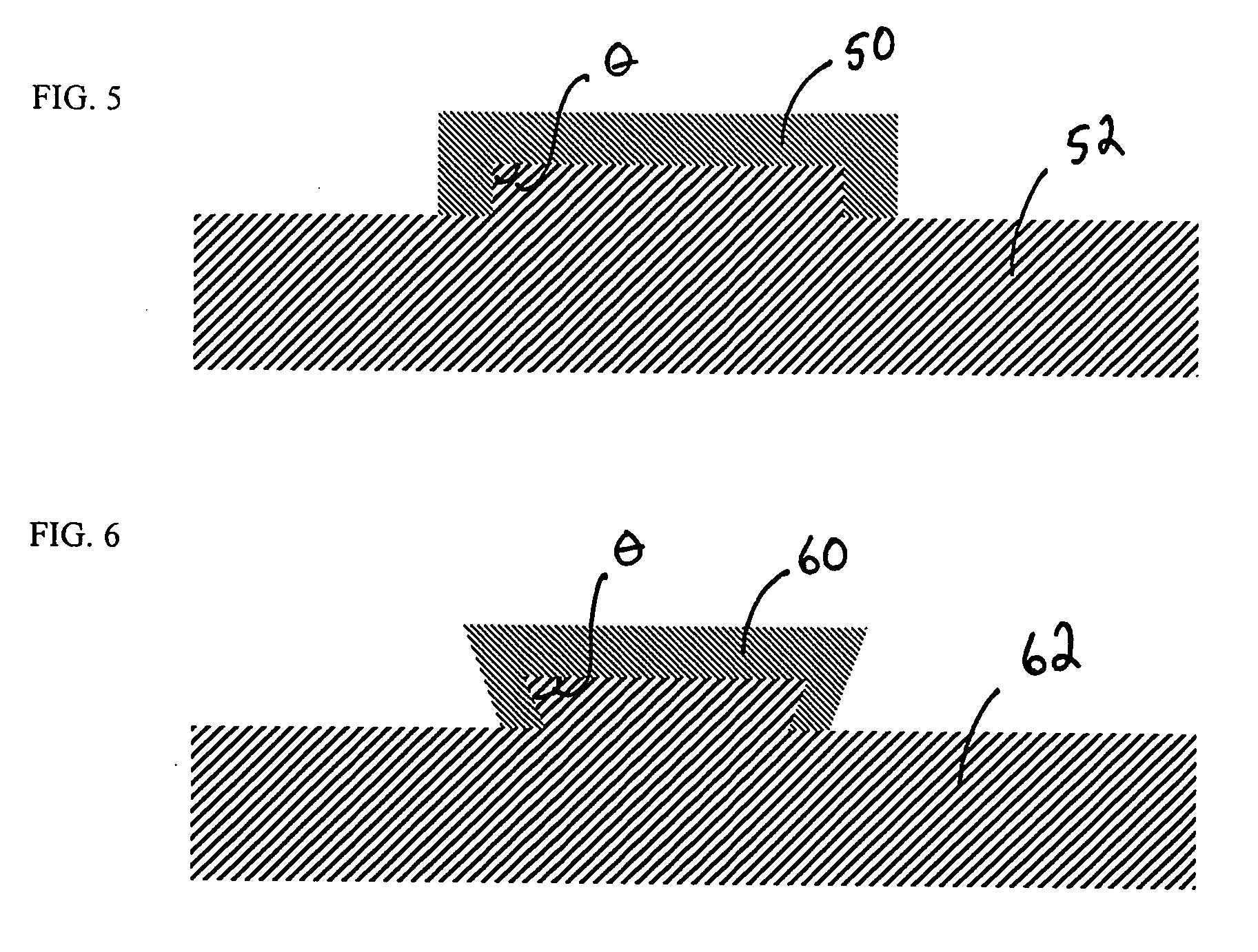
[0007]The present invention is a molded interconnect device having a high-current trace and a method for making a molded interconnect device with a high-current trace. In a first embodiment, the MID comprises a substrate surface and an interconnect pattern. The interconnect pattern is at least one of a rib raised from the substrate surface and a channel protruding into the substrate surface. The MID is preferably formed from a photosensitive material in a one-shot molding process. An interconnect path is written on at least a portion of the interconnect pattern and a trace is grown on the interconnect path, forming at least one of an angle and a curve in cross section. The interconnect path is preferably written by a laser or by a photolithography process.
[0008]In a second embodiment, the invention comprises the steps of molding a MID of a photosensitive plastic, the MID having a substrate surface and an interconnect pattern comprising at least one of a rib raised from the substrate surface and a channel protruding into the substrate surface, writing an interconnect path on at least a portion of a surface of the interconnect pattern, preferably by a laser...

Problems solved by technology

While the two-shot molding process works well, it is expensive and time-consuming.
The costs of the plating process usually limit increasing the depth of the trace.
A desire for smaller components and scarce space for applications usually limits the width of the trace.

Method used


Image

  • High-current traces on plated molded interconnect device
  • High-current traces on plated molded interconnect device
  • High-current traces on plated molded interconnect device

Examples


second embodiment

[0024]A high-current trace 30 of the present invention is shown in cross-sectional view in FIG. 3. Molded interconnect device 32 is preferably made of a photosensitive material by a one-shot molding process. MID 32 has an interconnect pattern that is a channel 34, having surfaces 34a, 34b, and 34c, which in this embodiment are flat, recessed into the substrate surface 36 of MID 32. In this embodiment, channel 34 is trapezoidal in cross-section. A conductive material 35, preferably copper, is grown on surfaces 34a, 34b, and 34c, which in this embodiment are flat, to create trace 30. Trace 30 is preferably grown by plating onto an interconnect path written on at least a portion of the interconnect pattern. The interconnect path has been written by a laser or other illuminator as described herein. Accordingly, while trace 30 has an apparent width relative to MID 32 that is approximately the same as the width of trace 10 of the prior art, and a depth of that is approximately the same as...

third embodiment

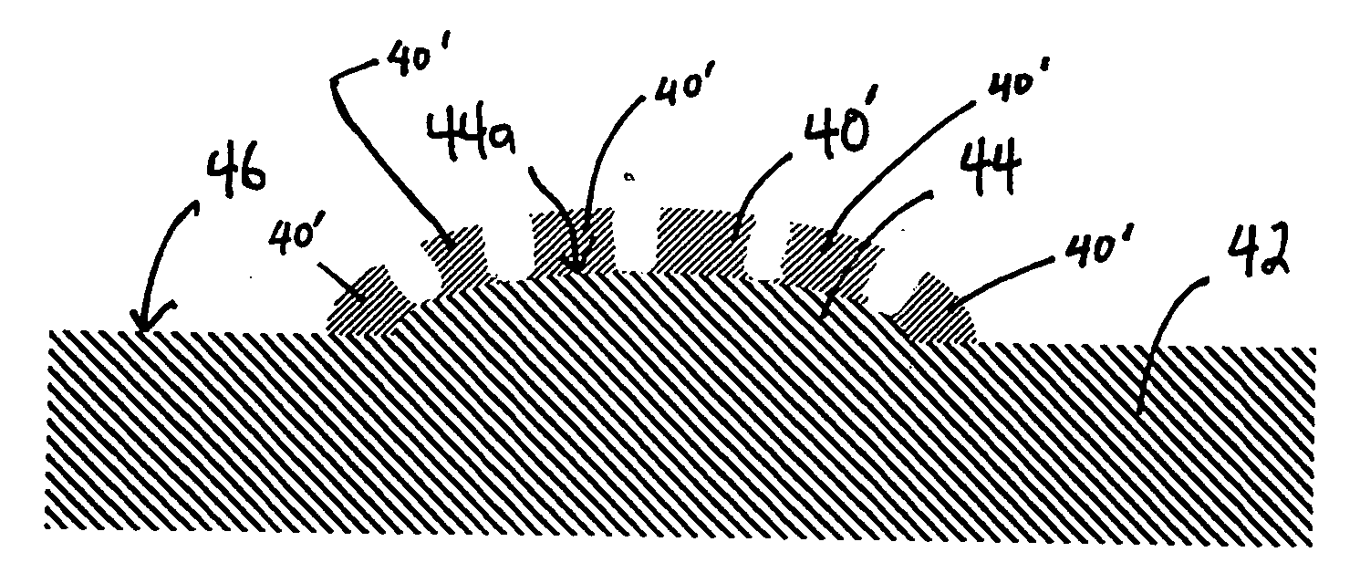
[0025]In yet another embodiment, a curved surface is used. A high-current trace 40 of the present invention is shown in cross-sectional view in FIG. 4. Molded interconnect device 42 is preferably made of a photosensitive material by a one-shot molding process. MID 42 has an interconnect pattern that is a raised rib 44 protruding from the substrate surface 46. In this embodiment, rib 44 is ovate in cross-section and has a surface 44a, which in this case is a single, curved surface. A conductive material 45, preferably copper, is grown on surface 44a, to create trace 40. Trace 40 is grown preferably by plating onto an interconnect path written on at least a portion of the interconnect pattern. The interconnect path has been written by a laser or other illuminator as described herein. Accordingly, while trace 40 has an apparent width relative to MID 42 that is approximately the same as the width of trace 10 of the prior art, and a depth of metal that is approximately the same as the de...

first embodiment

[0034]The interconnect path of trace 20 is then written on rib 24 (Step 103). In a first embodiment, a focused laser is used. The laser beam breaks the metal atoms from the organic ligands of the organic metal complex, or reduces the metal of the spinel-based metal oxide, and creates a microscopically irregular surface. The laser beam preferably writes the interconnect path on all three protruding sides 24a, 24b, 24c of rib 24. If necessary, MID 22 can be rotated, tilted, or otherwise oriented with respect to the laser source to ensure proper laser marking of all portions of surfaces to be plated. The laser beam can also write the interconnect path on only portions of the surface of rib 24 if desired for the end application.

[0035]MID 22 is next cleaned to remove debris (Step 105), preferably by use of demineralized water. Next, trace 20 is grown on the interconnect pattern by immersion of MID 22 in a current-free bath, preferably a current-free copper bath (Step 107). The metal will...


PUM

PropertyMeasurementUnit
Angleaaaaaaaaaa
Currentaaaaaaaaaa
Electrical conductoraaaaaaaaaa

Abstract

A molded interconnect device with a high-current trace and methods of making a molded interconnect device with a high-current trace are described. The molded interconnect device comprises a substrate surface and an interconnect pattern. The interconnect pattern is at least one of a rib raised from the substrate surface and a channel protruding into the substrate surface. In a first embodiment, the molded interconnect device is molded from photosensitive plastic molded in a one-shot molding process. A trace is grown on the portion of the interconnect pattern where an interconnect path has been written, either by a laser or by photolithography. In a second embodiment, the molded interconnect device is molded of plastic and the trace is grown by at least one of a mask and print-and-plate process and a mask and print-and-etch process. The trace forms at least one of an angle and a curve in cross section.

Description

FIELD OF THE INVENTION[0001]This invention relates to the field of molded interconnect devices [“MIDs”]. A MID has at least one electrical trace grown, usually by plating of a conductive metal, on a molded plastic structure. The trace carries data signals, control signals, or power to and from components of the application. MIDs are used in a variety of industries as, for examples, sensors, switches, connectors, instrument panels, and controllers.BACKGROUND OF THE INVENTION[0002]In the prior art, MIDs were created by molding part of a structure in one mold, using a first plastic material, then placing the structure in a second mold and shooting again with a second plastic material. The two plastic materials are selected so that a conductive material can be plated on one of the plastic materials and not on the other plastic material. The conductive material, grown on the platable plastic, becomes a trace. A representative method of two-shot molding is described in U.S. Pat. No. 5,359...

Claims


Application Information

Patent Timeline
IPC IPC(8): B32B3/00B29C59/00B29C41/22B29D31/00B32B15/08B29D99/00
CPCH05K1/0284H05K1/0373H05K3/107H05K3/185H05K2201/0209H05K2201/0236Y10T428/24802H05K2201/09045H05K2201/09118H05K2201/09981H05K2203/107Y10T428/24917H05K2201/09036
Inventor ZADEREJ, VICTOR
Owner MOLEX INC
Learn More