Multilayer capacitor

Active Publication Date: 2008-06-19
TDK CORPARATION
View PDF11 Cites 38 Cited by
  • Summary
  • Abstract
  • Description
  • Claims
  • Application Information

AI Technical Summary

Benefits of technology

[0015]The present invention was made in the view of such circumstance, and the object of the present invention is to provide a multilayer capacitor, not a multi-terminal capacitor, able to greatly reduce the ESL with low manufacturing cost.Means for Solving Problem
[0033]By connecting the first lead portion to the first terminal electrode formed straddling the first, the second and the third side faces, a current flow area of an electric current which flows between the first terminal electrode and the first conductor layers electrode becomes larger. As a result of this, the ESL of whole multilayer capacitor can be reduced.
[0034]By connecting the second lead portion to the second terminal electrode formed straddling the first, the second and the fourth side faces, a current flow area of an electric current which flows between the second terminal electrode and the second conductor layers becomes larger. As a result of this, the ESL of whole multilayer capacitor can be reduced.
[0036]In the multilayer capacitor according to the present invention, in case that said first terminal electrode and said second terminal electrodes are formed on said first side face and said second side face, any one of said first side face or said second side face may be installed to face a substrate. Namely, in the multilayer capacitor according to the present invention, installation directionality of multilayer capacitor to circuit substrate can be eliminated.
[0039]In the case of forming the dielectric body by stacking the dielectric layer, the first conductor layer and the second conductor layer, the first space pattern and the second space pattern are being as markers, interlayer can be aligned, and stacking misalignment can be prevented.

Problems solved by technology

Therefore, it has become extremely difficult to keep fluctuations in the power source voltage to within tolerances when faced with rapid changes in the load current.
Along with the increasingly higher operating frequencies of today's CPU's, however, the fluctuations in the load current have become faster and larger.
However, in the multi-terminal capacitor, there are problems that preparing a plurality of conductor layer patterns is necessary, and that increasing number of external terminals results in higher manufacturing cost.

Method used


Image

  • Multilayer capacitor
  • Multilayer capacitor
  • Multilayer capacitor

Examples


first embodiment

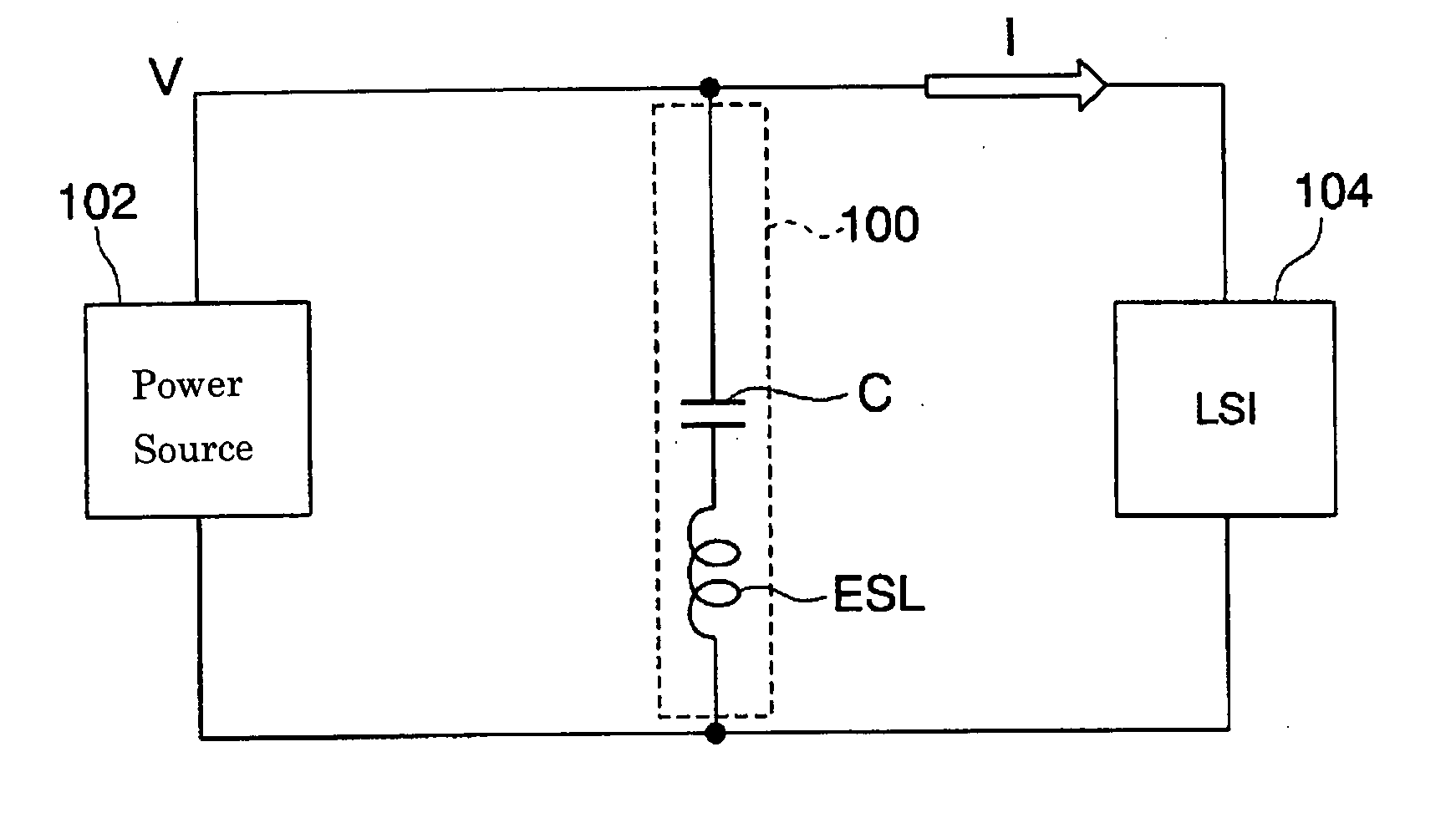
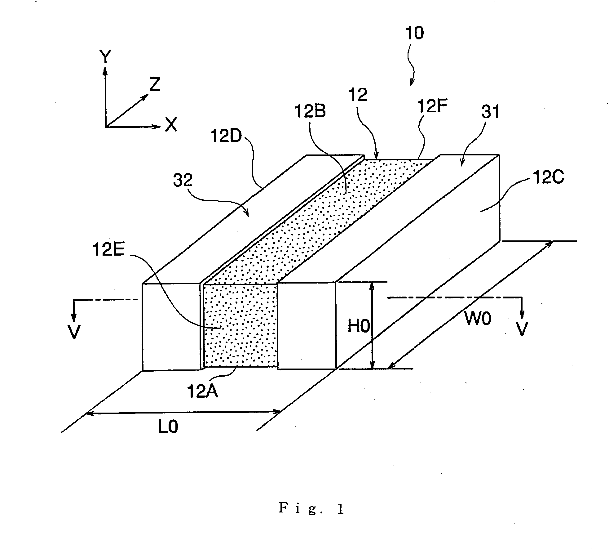
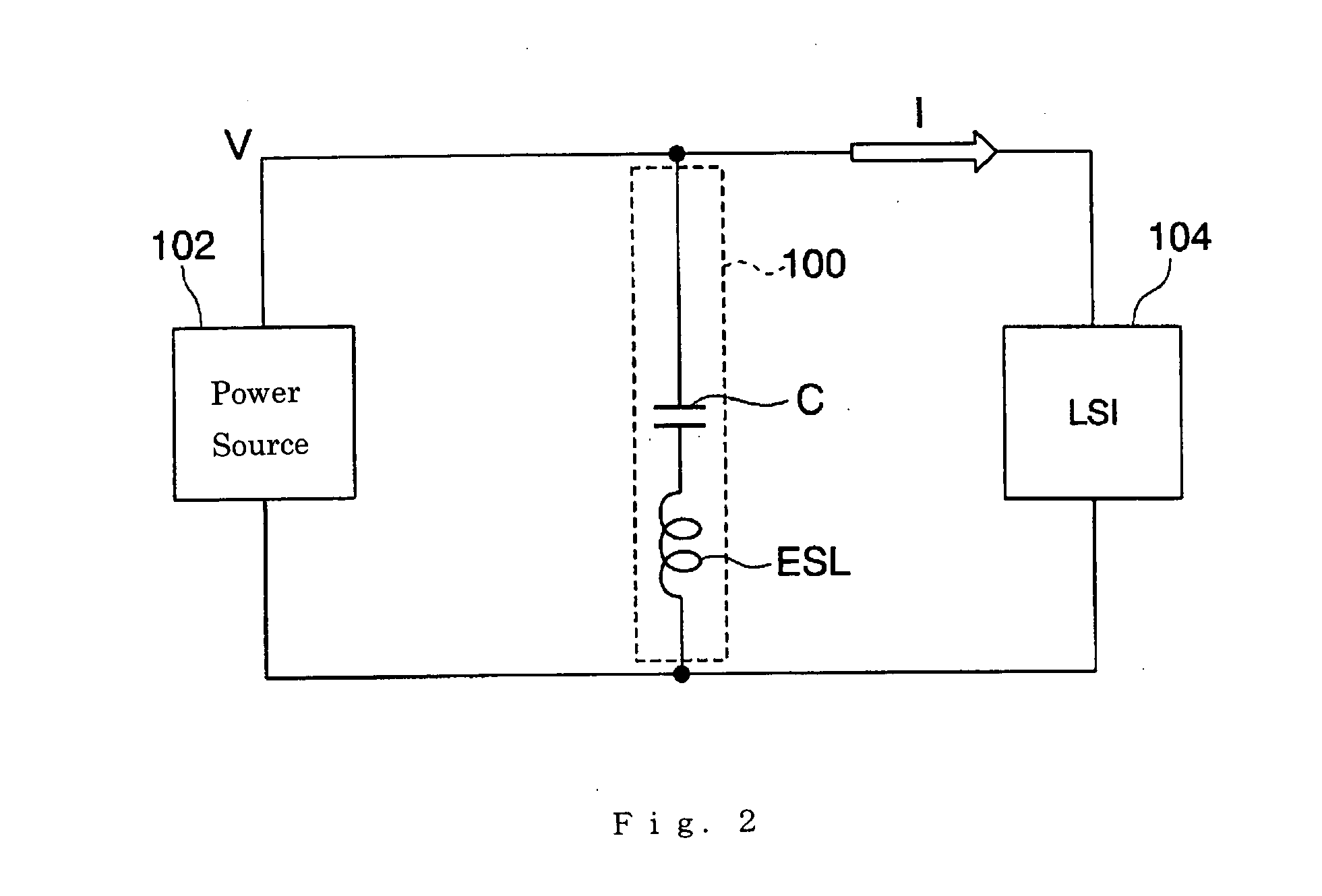
[0057]Whole constitution of a multilayer ceramic capacitor (herein after simply referred to as a “multilayer capacitor”) 10 of a first embodiment of the present invention is specified. As shown in FIG. 1, the multilayer capacitor 10 comprises a dielectric body 12, a rectangular parallelepiped shaped sintered body obtained by firing a stack of a plurality of ceramic green sheets as dielectric layers.

[0058]The dielectric body 12 comprises a first side face 12A and a second side face 12B opposed to the first side face. Also, the dielectric body 12 comprises a third side face 12C and a fourth side face 12D which are adjacent to the first side face 12A and the second side face 12B, and parallel to the stacking direction Z of the dielectric body, plus opposed to each other. The dielectric body also comprises a fifth side face 12E and a sixth side face 12F vertical to the stacking direction Z and opposed to each other.

[0059]In the present embodiment, preferably, as shown in FIG. 1, width L...

second embodiment

[0082]Next, a second embodiment of the present invention will be explained. Note that, in the following, explanation of common matters of the first embodiment and the second embodiment are omitted and only different points of both embodiments will be explained.

[0083]As shown in FIG. 6A, the first conductor layer 21 has a shape corresponding to an external shape of the dielectric layer 12a, and a first conductor layer main body portion 21a spaced with predetermined insulating space pattern 43 from circumference end portion of the dielectric layer 12a. This first conductor layer body portion 21a is a portion which composes one of an electrode of a capacitor. The first conductor layer 21 is formed on the same plane with the first conductor layer main body portion 21a integrally, and further comprises a first lead portion 21L led out straddling two adjacent side faces of the dielectric body 12 each other (the first side face 12A, the third side face 12C). In the first lead portion 21L, ...

third embodiment

[0089]Next, a third embodiment of the present invention will be explained. Note that, in the following, explanation of common matters of the first embodiment and the third embodiment are omitted and only different points of both embodiments will be explained.

[0090]In the present embodiment, as shown in FIG. 7A, in the first lead portion 21L, the first space pattern 41, which is not connected with said first terminal electrode 31, is formed at a position along with the third side face 12C.

[0091]In the case of stacking the dielectric body 12a, the first conductor layer 21 and the second conductor layer 22, in the third side face 12C, stacking misalignment can be prevented by arranging each of the first space pattern 41 in the stacking direction Z.

[0092]In the present embodiment, as shown in FIG. 7B, in the second lead portion 22L, the second space pattern 42, which is not connected with said second terminal electrode 32, is formed at a position along with the fourth side face 12D.

[009...


PUM


Abstract

A multilayer capacitor 10 comprising a dielectric body 12 having an approximately rectangular parallelepiped shape formed by alternately stacking a plurality of dielectric layer 12a, a first conductor layer 21, a second conductor layer 22, a first terminal electrode 31 and a second terminal electrode 32 formed on a first side face 12A of side faces 12 of the dielectric body in parallel to a stacking direction Z. The first conductor layer 21 comprises a first lead portion 21L connected to the first terminal electrode 31, the second conductor layer 22 comprises a second lead portion 22L connected to the second terminal electrode 32. Between a length “a” of the first lead portion 21L and the second lead portion 22L in vertical direction to the stacking direction Z, a length “b” of conductor layers positioned at both ends of the dielectric body 12 in the stacking direction, a space length “c” of the first side face 12A and the first conductor layer 21, a total number of the conductor layers 22, 22, (a+c) / (b×n)≦0.035 is consisted.

Description

BACKGROUND OF THE INVENTION[0001]1. Field of the Invention[0002]The present invention relates to multilayer capacitor greatly reducing the equivalent serial inductance (ESL) and production method thereof, more particularly relates to a multilayer capacitor used as a decoupling capacitor etc.[0003]2. Description of the Related Art[0004]In recent years, while advances have been made in reducing the voltage of power sources used for supplying power to large-scale integrated circuits (LSI's) and other integrated circuits, the load current has increased.[0005]Therefore, it has become extremely difficult to keep fluctuations in the power source voltage to within tolerances when faced with rapid changes in the load current. Therefore, as indicated in FIG. 2, a decoupling capacitor 100 (for example two-terminal structure multilayer ceramic capacitor) is now being connected to a power source 102. At the time of transitory fluctuation in the load current, current is supplied from this multila...

Claims


Application Information

Patent Timeline
IPC IPC(8): H01G4/30
CPCH01G4/30H01G4/232
Inventor TOGASHI, MASAAKI
Owner TDK CORPARATION
Why Eureka
Try Eureka