LCDS with integrated touch panels
a touch panel and touch panel technology, applied in the field of liquid crystal displays, can solve the problems of erroneous reporting of external pressure, common voltage distortion, and severe distortion of common voltage, and achieve the effect of eliminating coupling noise and preventing sensor malfunction
- Summary
- Abstract
- Description
- Claims
- Application Information
AI Technical Summary
Benefits of technology
Problems solved by technology
Method used
Image
Examples
first embodiment
[0053]A common electrode panel of the LCD according to the present invention is described in detail below with reference to FIGS. 4 through 5B.
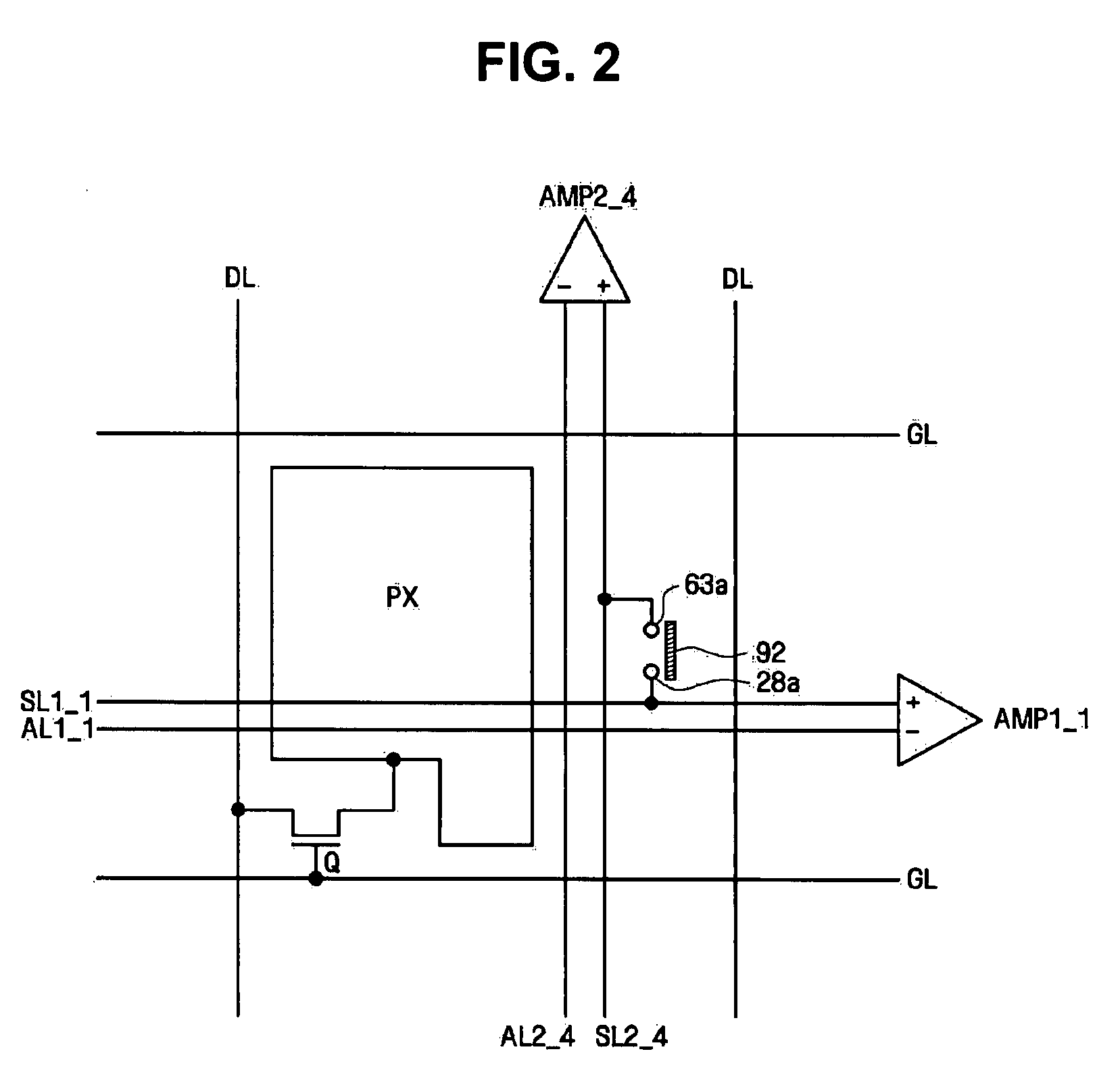
[0054]FIG. 4 is a partial plan view of a common electrode panel of the exemplary LCD of FIG. 1, showing a single, exemplary pixel thereof. FIG. 5A is a partial plan view of an exemplary LCD with an integrated touch panel including the TFT array panel of FIG. 3A and the common electrode panel of FIG. 4, showing a single, exemplary pixel thereof, and FIG. 5B is a partial cross-sectional view of the TFT array panel of FIG. 3A, as seen along the lines of the section Vb-Vb′ taken therein.
[0055]Referring to FIGS. 4 through 5B, a black matrix 94 for blocking light leakage, and a plurality of red, green and blue color filters 98 sequentially arranged on respective pixels are formed on an insulating substrate 96 preferably made of a transparent insulating material, such as glass. In the particular exemplary embodiment illustrated, a red color filter 9...
second embodiment
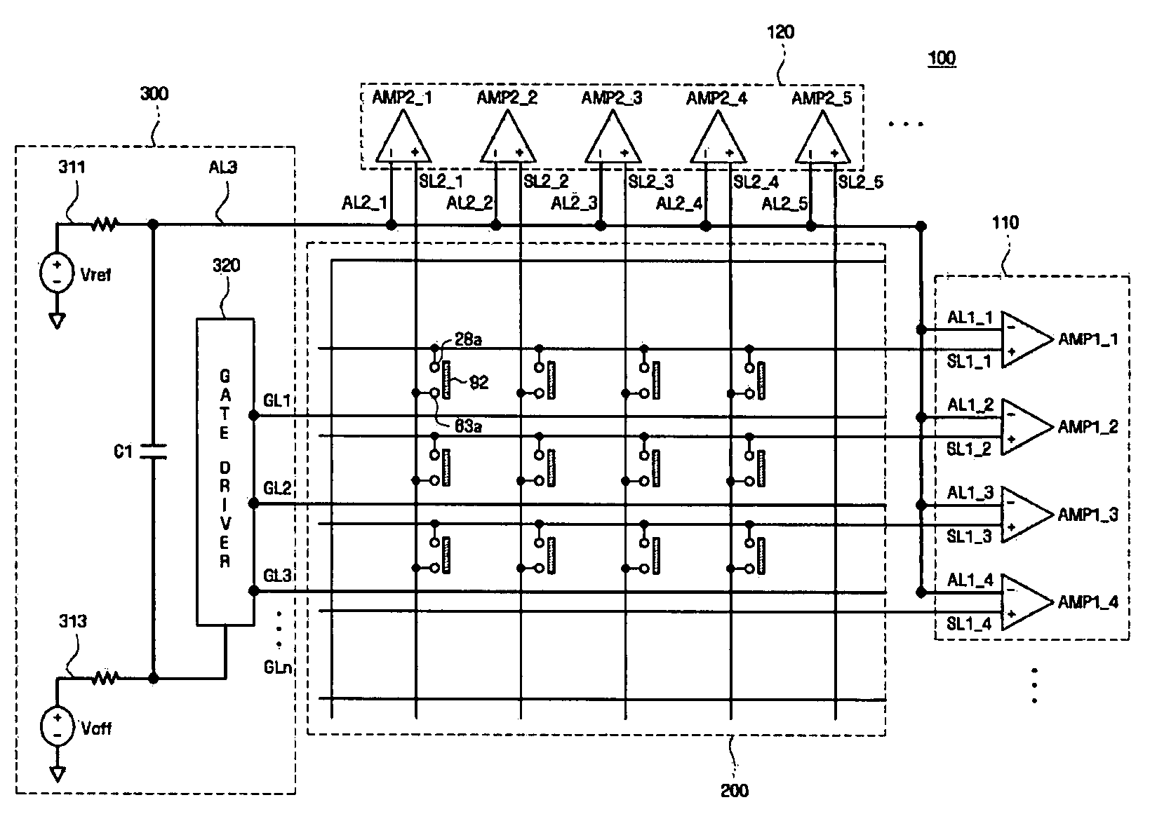
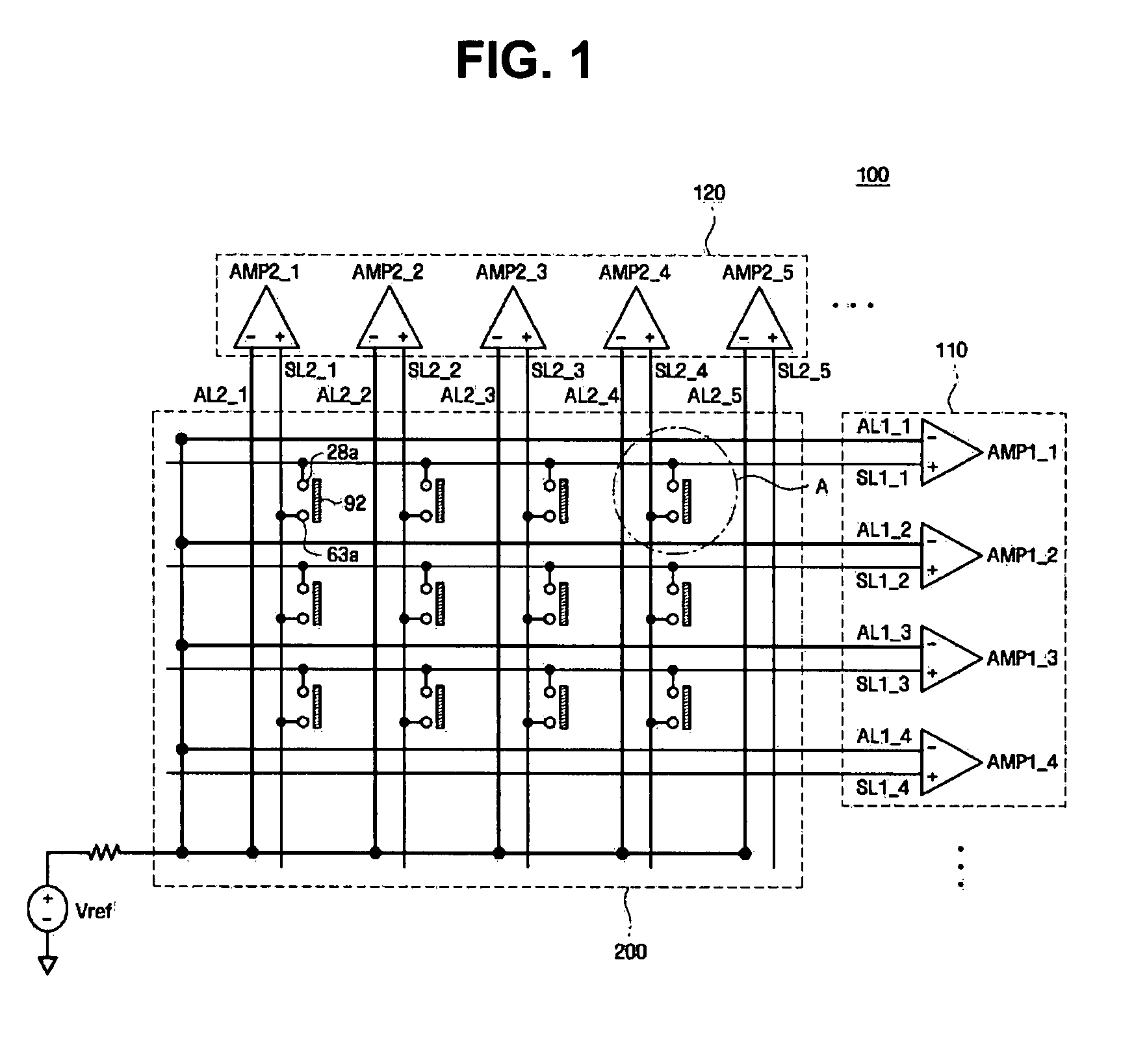
[0075]According to the third exemplary embodiment, which is a modification of the second embodiment, an initial voltage, which has been applied to the first and second sensor lines SL1_1 through SL1_4 and SL2_1 through SL2_5, is applied to the first, second and third dummy lines AL1, AL2_1 through AL2_4, and AL3_1 through AL3_5, and the third and fourth comparators AMP3_1 through AMP3_4 and AMP4_1 through AMP4_5 are connected to the output ports of the first and second comparators AMP1_1 through AMP1_4 and AMP2_1 through AMP2_5, respectively. The purpose of the foregoing arrangement is as follows.
[0076]When the initial voltage Vs, which has been applied to the first and second sensor lines SL1_1 through SL1_4 and SL2_1 through SL2_5, is applied to the first, second and third dummy lines AL1, AL2_1 through AL2_4, and AL3_1 through AL3_5, the voltage applied to the first and second sensor lines SL1_1 through SL1_4 and SL2_1 through SL2_5 and the voltage applied to the first, second an...
PUM
| Property | Measurement | Unit |
|---|---|---|
| area | aaaaa | aaaaa |
| reference voltage | aaaaa | aaaaa |
| voltage | aaaaa | aaaaa |
Abstract
Description
Claims
Application Information
 - R&D
- Intellectual Property
- Life Sciences
- Materials
- Tech Scout
- Unparalleled Data Quality
- Higher Quality Content
- 60% Fewer Hallucinations
Browse by: Latest US Patents, China's latest patents, Technical Efficacy Thesaurus, Application Domain, Technology Topic, Popular Technical Reports.
© 2025 PatSnap. All rights reserved.Legal|Privacy policy|Modern Slavery Act Transparency Statement|Sitemap|About US| Contact US: help@patsnap.com


