
Package substrate having embedded capacitor

a technology of capacitors and substrates, applied in the field of packaging substrates, can solve the problems of discrete capacitors b>130/b> easily damaged or broken, and hardly enhance the performance of a conventional circuit substrate, and achieve the effect of enhancing space and degree of freedom

Inactive Publication Date: 2008-05-29
UNIMICRON TECH CORP
View PDF5 Cites 24 Cited by
  • Summary
  • Abstract
  • Description
  • Claims
  • Application Information

AI Technical Summary

Benefits of technology

[0008]Accordingly, the present invention directs to a package substrate having embedded capacitor for enhancing the space and degree of freedom of disposing the embedded capacitor.
[0009]The present invention also directs to a package substrate having embedded capacitor such that the performance of the package substrate is enhanced by using a dielectric material with high dielectric constant and low dielectric loss.
[0010]The present invention directs to a package substrate having embedded capacitor such that the embedded capacitor is protected from damage by covering it with a passivation layer.
[0018]Due to the improvement in the substrate structure, the embedded capacitor in the present invention can be disposed in a suitable location without having to avert the conductive through hole. Therefore, the space and degree of freedom for disposing the embedded capacitors is enhanced. In addition, capacitors fabricated using high dielectric constant and low dielectric loss material such as polymer-ceramic composite can be used instead of the conventional discrete capacitors so as to enhance the performance of the package substrate. Furthermore, the embedded capacitors of the present invention is covered with at least one passivation layer to prevent the embedded capacitors from receiving possible damage in the process of compressing the substrate. Hence, overall reliability of the package substrate is improved.

Problems solved by technology

However, because the capacitance of the conventional discrete capacitor is low and has a low dielectric constant, they could hardly enhance the performance of a conventional circuit substrate.
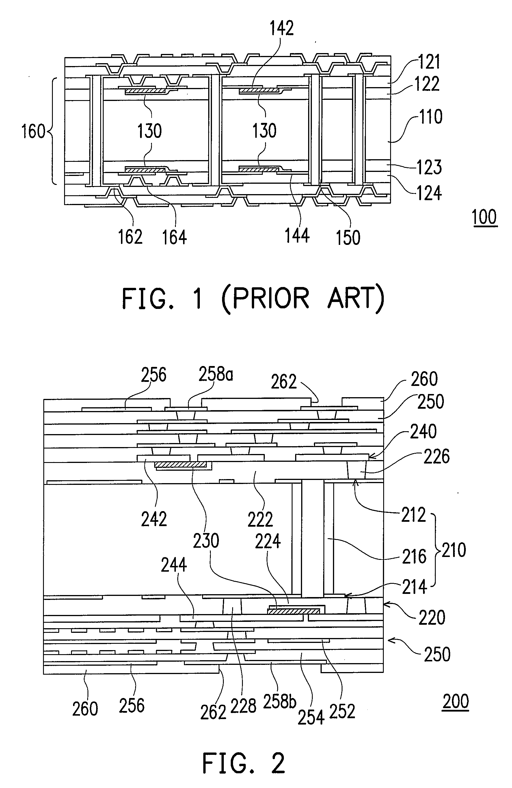
In the meantime, the discrete capacitors 130 are easily damaged or broken in the process of compressing the substrate.

Method used


Image

  • Package substrate having embedded capacitor
  • Package substrate having embedded capacitor
  • Package substrate having embedded capacitor

Examples


first embodiment

[0028]FIG. 2 is a schematic diagram of a portion of a package substrate having embedded capacitor according to the present invention. The package substrate 200 mainly includes a core circuit board 210, a dielectric layer 220, at least one embedded capacitor 230 and a metal layer 240. The core circuit board 210 is, for example, a copper foil substrate with glass fiber and epoxy resin serving as insulating material so as to enhance the strength and support of the package substrate 200. In addition, the core circuit board 210 has at least one conductive through hole 216. The method of forming the conductive through hole 216 includes, for example, performing a mechanical drilling to form a through hole and then performing an electrochemical plating to form a layer of conductive material on the inner sidewall of the through hole. As a result, the upper and lower copper foils are connected through the conductive through hole 216. After an etching operation is performed to pattern the copp...

second embodiment

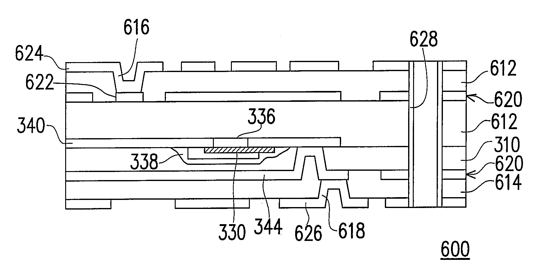
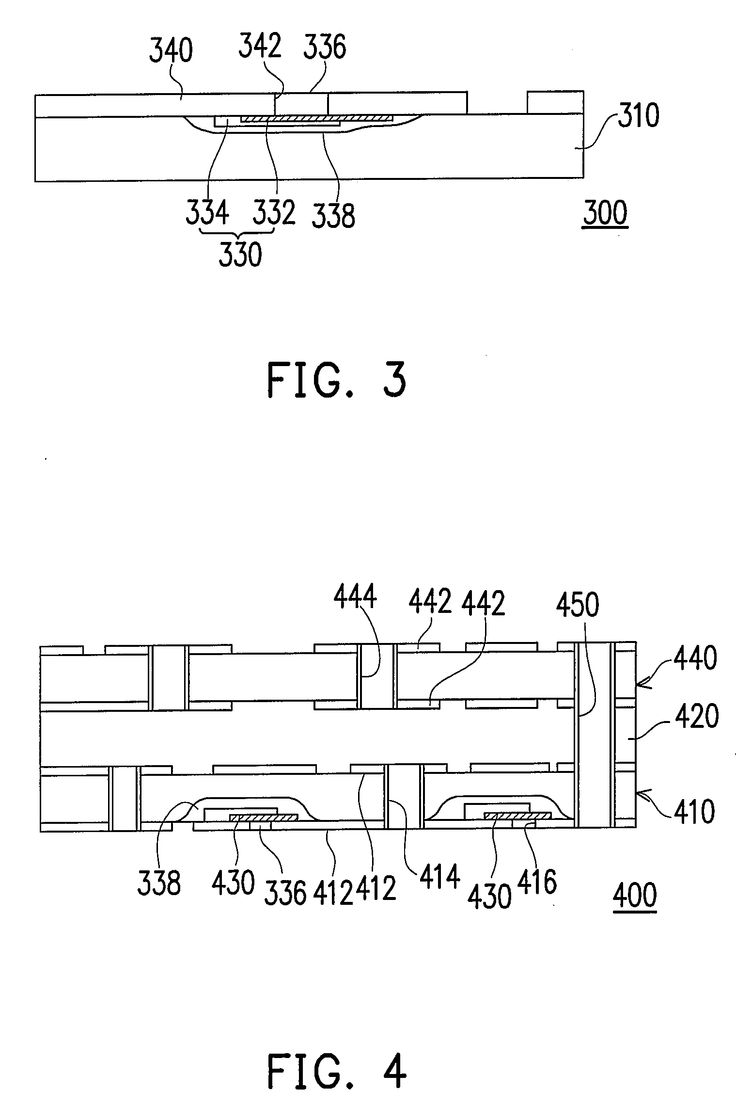
[0033]FIG. 3 is a schematic diagram of a portion of a package substrate having embedded capacitor according to the present invention. The package substrate 300 mainly includes a core board 310, at least one embedded capacitor 330, a first passivation layer 338 and a metal layer 340. The core board 310 is a substrate fabricated using glass fibers and epoxy resin as its insulating material so as to enhance the strength and support of the package substrate 300. In addition, the embedded capacitor 330 is embedded in the core board 310 and electrically connected to the metal layer 340. In the present embodiment, the embedded capacitor 330 can be an epoxy resin-ceramic composite capacitor or other ceramic / polymer composite capacitor with high dielectric constant formed on the metal layer 340 after performing a high-temperature sintering process. Afterwards, electrode material covers the dielectric material 332 to form an electrode 334 connected to the metal layer 340.

[0034]To prevent the ...

third embodiment

[0035]FIG. 4 is a schematic diagram of a portion of a package substrate having embedded capacitor according to the present invention. The package substrate 400 mainly includes a first core circuit board 410, a dielectric layer 420, at least one embedded capacitor 430 and a second core circuit board 440. The first and second core circuit boards 410 and 440 are, for example, copper foil substrates using glass fiber or epoxy resin as the insulating material so as to enhance the strength and support of the package substrate 400. In addition, the dielectric layer 420 can be cured or semi-cured glass fiber epoxy resin laminated between the first and the second core circuit board 410 and 440. In the present embodiment, the two opposing surfaces of the first core circuit board 410 have a metal layer 412 and at least one first conductive through hole 414 of the first core circuit board 410 is connected to the metal layer 412. The embedded capacitor 430 is embedded in the first core circuit b...


PUM


Abstract

A package substrate having embedded capacitor is provided. The package substrate includes a first core circuit board, at least one embedded capacitor, a second core circuit board and a dielectric layer. At least one metal layer is disposed on a surface of the first core circuit board and at least one first conductive through hole of the first core circuit board is connected to the metal layer. The embedded capacitor is embedded in the first core circuit board and connected to the metal layer. A wiring layer is disposed on a surface of the second core circuit board and at least one second conductive through hole of the second core circuit board is connected to the wiring layer. The dielectric layer is laminated between the first and the second core circuit boards.

Description

CROSS-REFERENCE TO RELATED APPLICATION[0001]This application claims the priority benefit of Taiwan application serial no. 95141129, filed Nov. 7, 2006. All disclosure of the Taiwan application is incorporated herein by reference.BACKGROUND OF THE INVENTION[0002]1. Field of the Invention[0003]The present invention relates to a package substrate, and more particularly to a package substrate having embedded capacitor.[0004]2. Description of Related Art[0005]Embedded capacitor can be integrated into a package substrate in the same fabrication process to enhance the efficiency of the active components inside an electronic package, improve electrical performance and lower assembling cost. Therefore, it has become the mainstream method for fabricating electronic carrier. At present, the development of embedded capacitor is mainly aiming toward small size ceramic capacitors. In general, ceramic capacitors can be classified into single layer ceramic capacitors (SLCC) and multi-layer ceramic ...

Claims


Application Information

Patent Timeline
Patent Type & Authority Applications(United States)
IPC IPC(8): H05K1/16
CPCH05K1/162H05K3/4602H05K3/4623H05K2201/09763H05K2201/0355H05K2201/09536H05K3/4644
Inventor FAN, CHIH-PENG
Owner UNIMICRON TECH CORP
Learn More