Optical transceiver and method of controlling optical output jitter using the same

a technology of optical output and optical transceiver, which is applied in the direction of duplex signal operation, amplitude demodulation, instruments, etc., can solve the problems of smaller module size, reduce the size of the module, and reduce the jitter of optical outpu

Active Publication Date: 2008-05-08
ELECTRONICS & TELECOMM RES INST
View PDF5 Cites 24 Cited by
  • Summary
  • Abstract
  • Description
  • Claims
  • Application Information

AI Technical Summary

Benefits of technology

[0019]Such EQ filter is a passive type filter, and the passive type EQ filter blocks low-frequency components, thereby reducing optical output jitter.
[0020]According to another aspect of the present invention, there is provided a method of controlling optical output jitter using the optical transceiver described above, the method including: reducing jitter of a high speed electric signal, wherein when the optical transceiver is a XFP transceiver (10 Gb / s Small Form-factor Pluggable), the transmitter unit comprises a Clock and Data Recovery (CDR) unit, and a Laser Diode (LD) driver, and a Transmitter Optical Sub-Assembly (TOSA), and the EQ filter is interposed between the CDR unit and the LD driver, and when the optical transceiver is a 300-pin Multi-Source Agreement (MSA) transceiver, the transmitter unit comprises a serializer, the LD driver, a Laser Diode (LD) module, and the EQ filter is interposed between the serializer and the LD driver.
[0021]The EQ filter may include: a receiver which receives an electric signal from the CDR unit or the serializer; an output driver which directly receives the signal outputted from the receiver; and a pre-emphasis driver which receives the signal outputted from the receiver through a delay device, wherein the optical transceiver comprises a filter control circuit that is connected to the micro-controller to control the EQ filter and the EQ filter amplifies high-frequency component, thereby reducing optical output jitter.
[0022]In addition, the EQ filter is embodied as at least one high pass filter, and when the EQ filter is embodied by two or more high pass filters, each filter is connected in series, wherein the EQ filter blocks high-frequency component using the EQ filter and thus optical output jitter may be reduced.

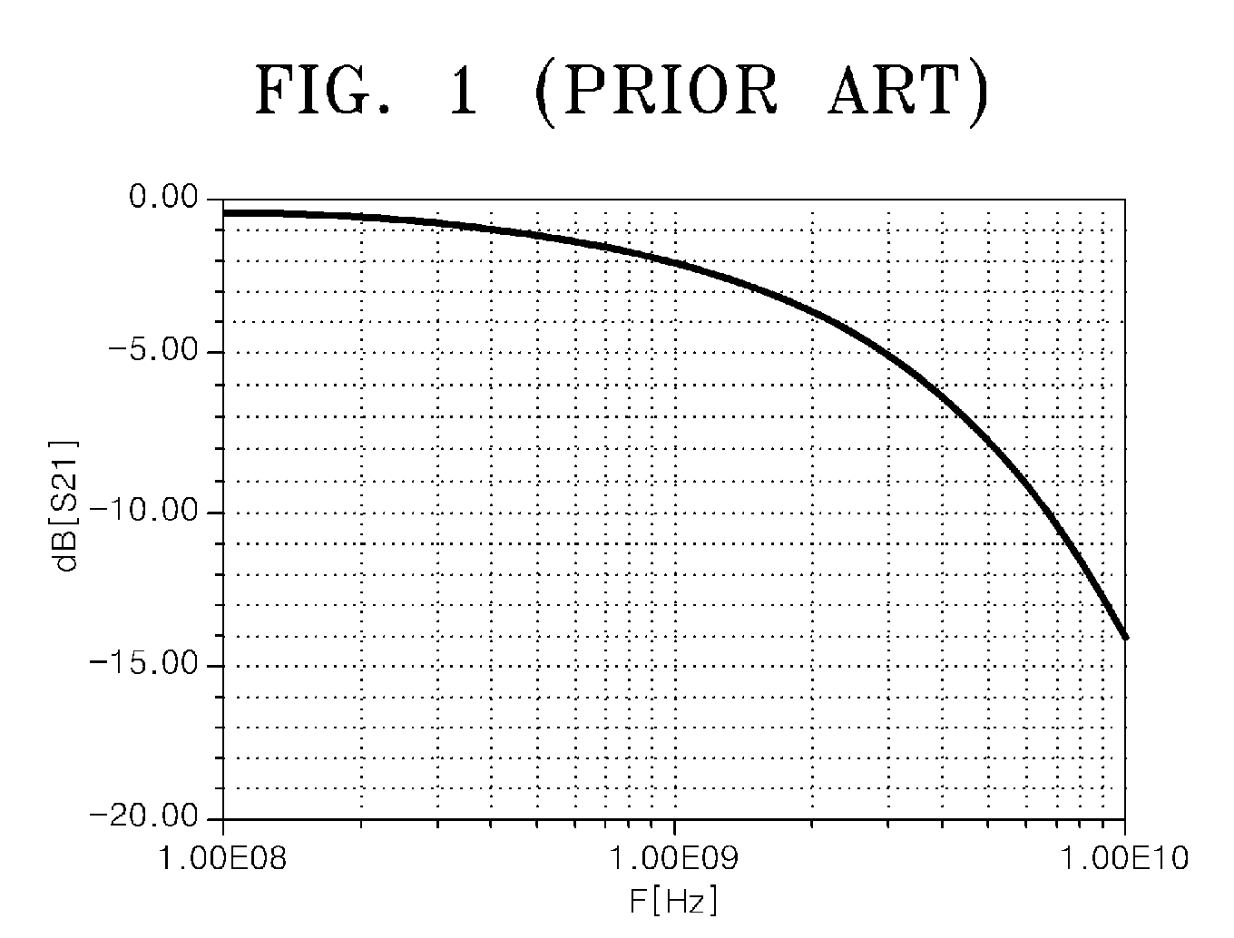
Problems solved by technology

Due to increases in speed of the optical communication devices, optical transmission speed of the optical transceiver has increased to over 10 Gb / s, however, the size of the module has become smaller.
In addition, if an impedence matching among a package of a chip, a Packet Assembly / Disassembly (PAD), and a transmission line is not well accomplished, reflection of high-frequency component greatly occurs and thus causes jitter.

Method used


Image

  • Optical transceiver and method of controlling optical output jitter using the same
  • Optical transceiver and method of controlling optical output jitter using the same
  • Optical transceiver and method of controlling optical output jitter using the same

Examples


Embodiment Construction

[0031]Hereinafter, the present invention will be described more fully with reference to the accompanying drawings, in which exemplary embodiments of the invention are shown. The invention may, however, be embodied in many different forms and should not be construed as being limited to the embodiments set forth herein; rather, these embodiments are provided so that this disclosure will be thorough and complete, and will fully convey the concept of the invention to those skilled in the art. In the drawings, like reference numerals denote like elements, and the sizes and thicknesses of layers and regions are exaggerated for clarity. Also, the terms used herein are defined according to the functions of the present invention. Thus, the terms may vary depending on users or operators and usages. That is, the terms used herein must be understood based on the descriptions made herein.

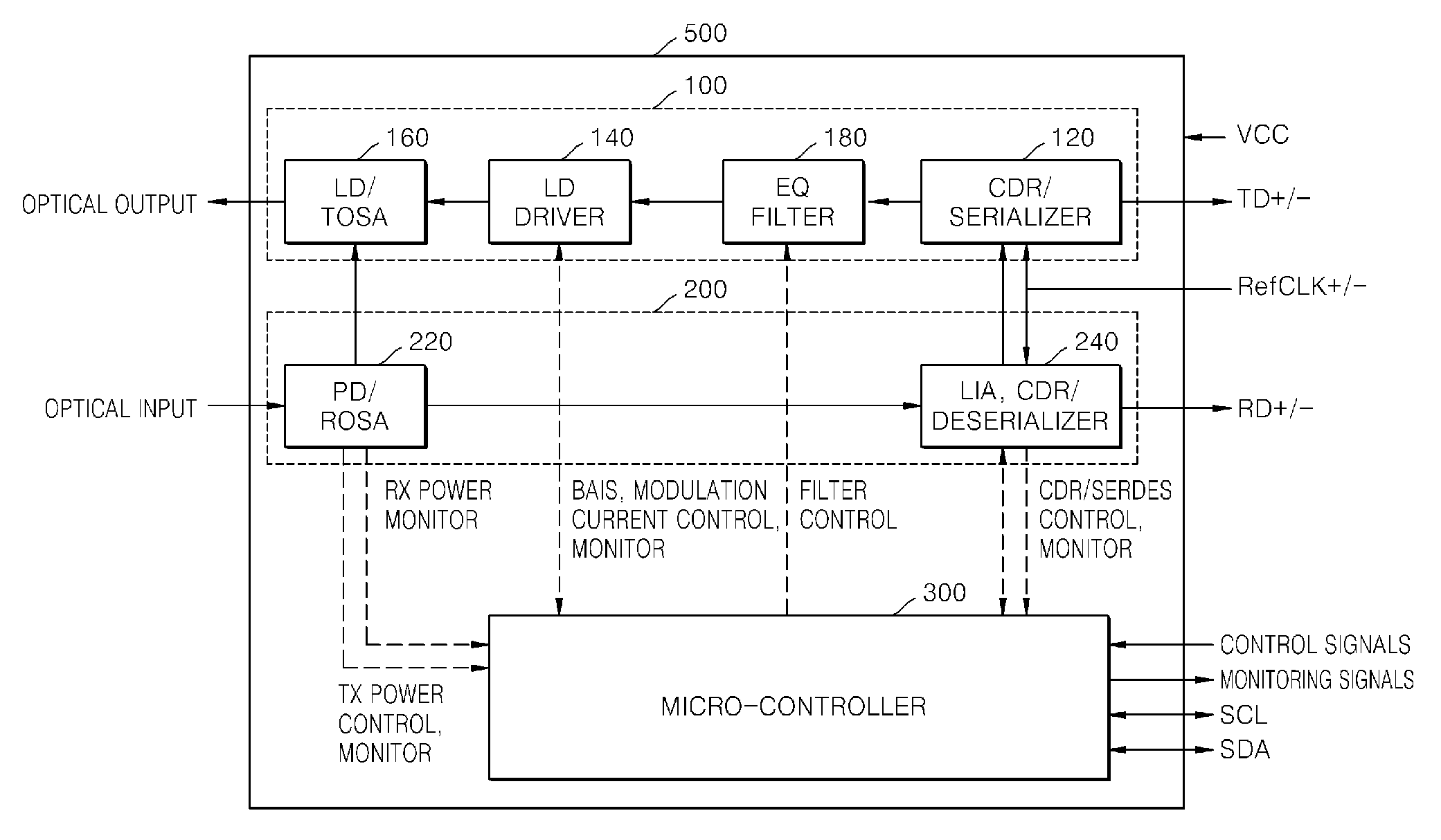
[0032]FIG. 3 is a block diagram schematically illustrating an optical transceiver according to an embodiment ...


PUM


Abstract

An optical transceiver which can effectively reduce optical output jitter when an error is made during designing and manufacturing of a printed circuit board (PCB), and a method of controlling optical output jitter using the optical transceiver are provided. The optical transceiver includes a transmitter unit including an equalizing (EQ) filter which can reduce jitter of a high speed electric signal; a control circuit which controls the EQ filter; a receiver unit which receives an optical signal; and a micro-controller which controls the transmitter unit and the receiver unit. Further included in the optical transceiver is an active type or passive type EQ filter and, in the case of the active type, the control circuit is used to control the filter, in order to compensate for high-frequency component of a high speed electric signal in the transmitter unit in order to reduce reflection or loss on the PCB, and thus deterministic optical output jitter occurring due to Inter-Symbol Interference (ISI) can be reduced.

Description

CROSS-REFERENCE TO RELATED PATENT APPLICATION[0001]This application claims the benefit of Korean Patent Application No. 10-2006-0109071, filed on Nov. 6, 2006, in the Korean Intellectual Property Office, the disclosure of which is incorporated herein in its entirety by reference.BACKGROUND OF THE INVENTION[0002]1. Field of the Invention[0003]This work was supported by the IT R&D program of MIC / IITA. [2006-S-059-01, ASON based Metro Photonic Cross-Connect Technology][0004]The present invention relates to an optical communication device, and more particularly, to an optical transceiver which can control optical output jitter and a method of controlling optical output jitter using the optical transceiver.[0005]2. Description of the Related Art[0006]An optical transceiver is a communication module which carries out optical-electric conversion and electric-optical conversion in an optical communication system. Due to increases in speed of the optical communication devices, optical transm...

Claims


Application Information

Patent Timeline
Patent Type & Authority Applications(United States)
IPC IPC(8): H04B10/00
CPCH04L25/03343H04B10/40H04B10/00
Inventor LEE, JOON KILEE, JYUNG CHANKIM, KWANGJOON
Owner ELECTRONICS & TELECOMM RES INST
Why Eureka
Try Eureka