Luminescent sheet having see-through property, luminescent decorative material, and method of producing luminescent sheet
a technology of luminescent decorative materials and luminescent sheets, which is applied in the field of luminescent sheets, can solve the problems of special-purpose decorative materials produced by the above methods, which are only visible in the daytime or under lighting, and are invisible at nigh
- Summary
- Abstract
- Description
- Claims
- Application Information
AI Technical Summary
Benefits of technology
Problems solved by technology
Method used
Image
Examples
example 1
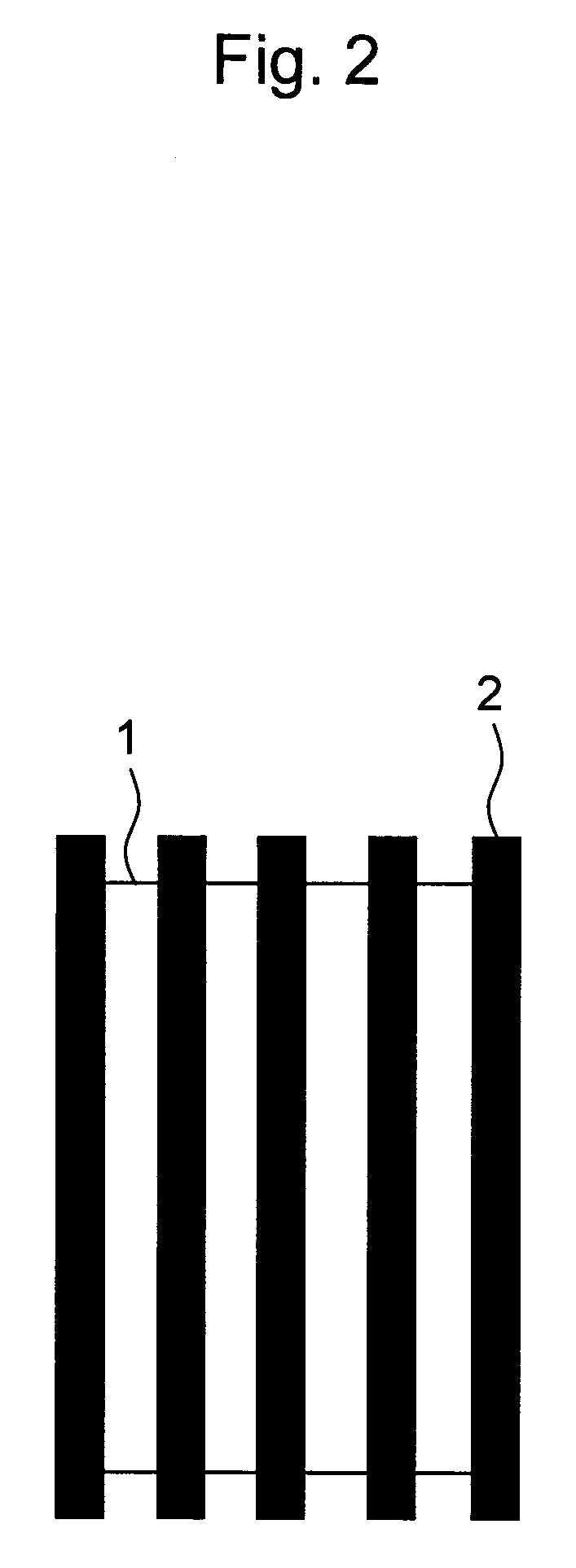
[0054] As shown in FIG. 2, masking tape 2 (1 cm in width and 20 μm in thickness, Adwill C-902, Lintec Corporation) was applied at 1-cm intervals in a length direction to a polyethylene terephthalate sheet 100 μm in thickness (DIAFOIL T-100, Mitsubishi Polyester Film Corporation) (FIG. 2) serving as a 1st transparent substrate 1. Then, a 1st transparent electrode layer 3 of 100 nm in thickness was formed in stripe pattern by sputtering with ITO (FIG. 3).
[0055] Further, masking tape 2′ (1 cm in width and 20 μm in thickness) similar to the above masking tape was applied thereto at 1-cm intervals in perpendicular direction (FIG. 4).
[0056] Subsequently, a ZnS:Cu solution (FEL-190, Fujikura Kasei Co., Ltd.) was coated thereto using a Mayer bar such that a luminescent layer 4 was formed to have a dried thickness of 40 μm (FIG. 5). Then, masking tape 2 and masking tape 2′ were removed therefrom (FIG. 6).
[0057] Masking tape 2 (1 cm in width and 20 μm in thickness, Adwill C-902, Lintec Cor...
example 2
[0060] As shown in FIG. 2, masking tape 2 (1 cm in width and 20 μm in thickness, Adwill C-902, Lintec Corporation) was applied at 1-cm intervals in a length direction to a polyethylene terephthalate sheet 100 μm in thickness (DIAFOIL T-100, Mitsubishi Polyester Film Corporation) (FIG. 2) serving as a 1st transparent substrate 1. Then, a 1st transparent electrode layer 3 of 100 nm in thickness was formed in stripe pattern by sputtering with ITO (FIG. 3).
[0061] Further, masking tape 2′ (1 cm in width and 20 μm in thickness) similar to the above masking tape was applied thereto at 1-cm intervals in perpendicular direction (FIG. 4).
[0062] Subsequently, a ZnS:Cu solution (FEL-190, Fujikura Kasei Co., Ltd.) was coated thereto using a Mayer bar such that a luminescent layer 4 (FIG. 5) was formed to have a dried thickness of 40 μm. After drying using a dryer at 100° C. for 30 minutes, a barium titanate solution (FEL-615, Fujikura Kasei Co., Ltd.) was further coated thereto such that a die...
example 3
[0067] A luminescent sheet was obtained in a manner similar to that used in Example 2, except that printing was carried out on a luminescent layer (ZnS:Cu), a dielectric layer (barium titanate solution), and a see-through control layer (conductive paste) using a screen printing method instead of masking tape.
[0068] As shown in FIG. 11, an AC voltage of 100 V with a frequency of 1000 Hz was applied to the thus obtained luminescent sheet in the direction of the sheet's thickness via voltage connection. As a result, the luminescent sheet was confirmed to be excellent in visibility even at night and further to have effects whereby it was possible to see therethrough from one side thereof while it was difficult to see therethrough from the other side thereof.
PUM
| Property | Measurement | Unit |
|---|---|---|
| Transparency | aaaaa | aaaaa |
| Luminescence | aaaaa | aaaaa |
Abstract
Description
Claims
Application Information
 - R&D
- Intellectual Property
- Life Sciences
- Materials
- Tech Scout
- Unparalleled Data Quality
- Higher Quality Content
- 60% Fewer Hallucinations
Browse by: Latest US Patents, China's latest patents, Technical Efficacy Thesaurus, Application Domain, Technology Topic, Popular Technical Reports.
© 2025 PatSnap. All rights reserved.Legal|Privacy policy|Modern Slavery Act Transparency Statement|Sitemap|About US| Contact US: help@patsnap.com


