
Capacitor, manufacturing method of the same, and electronic substrate including the same

a manufacturing method and capacitor technology, applied in the direction of variable capacitor details, fixed capacitor details, printed circuit non-printed electric components association, etc., can solve the problems of increased manufacturing cost, increased material cost, and difficulty in reducing the distance between the terminals and the wiring length

Inactive Publication Date: 2008-03-20
FUJITSU LTD
View PDF3 Cites 29 Cited by
  • Summary
  • Abstract
  • Description
  • Claims
  • Application Information

AI Technical Summary

Benefits of technology

[0015] In an embodiment of the invention which solves or reduces one or more of the above-mentioned problems, there is provided a capacitor including: a substrate; a conductive layer provided on the substrate and containing conductive compounds; a valve metal sheet having a dielectric part formed throughout an entire surface of the conductive layer; a protection layer covering the valve metal sheet; a first electrode terminal electrically connected to the conductive layer and partially exposed from an external surface of the protection layer; and a second electrode terminal electrically connected to a surface of the valve metal sheet which is opposite to a surface of the valve metal sheet on which the dielectric part is provided, and the second electrode terminal partially exposed from the external surface of the protection layer; wherein the dielectric part is made of an oxide of a metallic material of the valve metal sheet, the dielectric part is formed with an uneven surface on the conductive layer, and the conductive compounds of the conductive layer are in contact with the uneven surface of the dielectric part.
[0016] In an embodiment of the invention which solves or reduces one or more of the above-mentioned problems, there is provided a manufacturing method of a capacitor, the method including the steps of: forming a dielectric part by oxidizing an entire first surface of a valve metal sheet; forming a through hole in the valve metal sheet in which the dielectric part is formed; applying an adhesive conductive material to a surface of a substrate; attaching the valve metal sheet in which the through hole is formed, to the substrate so that the first surface contacts the conductive material on the substrate surface; forming a conductive layer by curing the conductive material; forming a protection layer which covers a second surface of the valve metal sheet which is opposite to the first surface of the valve metal sheet; forming openings in the protection layer, so that the conductive layer in the through hole and the second surface of the valve metal sheet are partially exposed from the openings; and filling up the openings in the protection layer with another conductive material to form electrode terminals.
[0017] In an embodiment of the invention which solves or reduces one or more of the above-mentioned problems, there is provided an electronic substrate including a capacitor, a semiconductor device, and a wiring substrate provided to connect the capacitor and the semiconductor device electrically, wherein the capacitor comprises: a substrate; a conductive layer provided on the substrate and containing conductive particles ; a valve metal sheet having a dielectric part formed throughout an entire surface of the conductive layer; a protection layer covering the valve metal sheet; a first electrode terminal electrically connected to the conductive layer and partially exposed from an external surface of the protection layer; and a second electrode terminal electrically connected to a surface of the valve metal sheet which is opposite to a surface of the valve metal sheet on which the dielectric part is provided, and the second electrode terminal partially exposed from the external surface of the protection layer; wherein the dielectric part is made of an oxide of a metallic material of the valve metal sheet, the dielectric part is formed with an uneven surface on the conductive layer, and the conductive particles of the conductive layer are in contact with the uneven surface of the dielectric part.

Problems solved by technology

In the case of the solid electrolytic capacitor, it is difficult to make small the distance between the terminals and the wiring length due to the structure thereof.
For this reason, the manufacturing cost is increased.
For this reason, the material cost is also increased.
Because of the above factors, it is difficult to attain low-cost manufacturing of the thin-film capacitor.
For this reason, the manufacturing processes are complicated, and it is difficult to attain low-cost manufacturing of the solid electrolytic capacitor.

Method used


Image

  • Capacitor, manufacturing method of the same, and electronic substrate including the same
  • Capacitor, manufacturing method of the same, and electronic substrate including the same
  • Capacitor, manufacturing method of the same, and electronic substrate including the same

Examples


Embodiment Construction

[0036] A description will now be given of an embodiment of the invention with reference to the accompanying drawings.

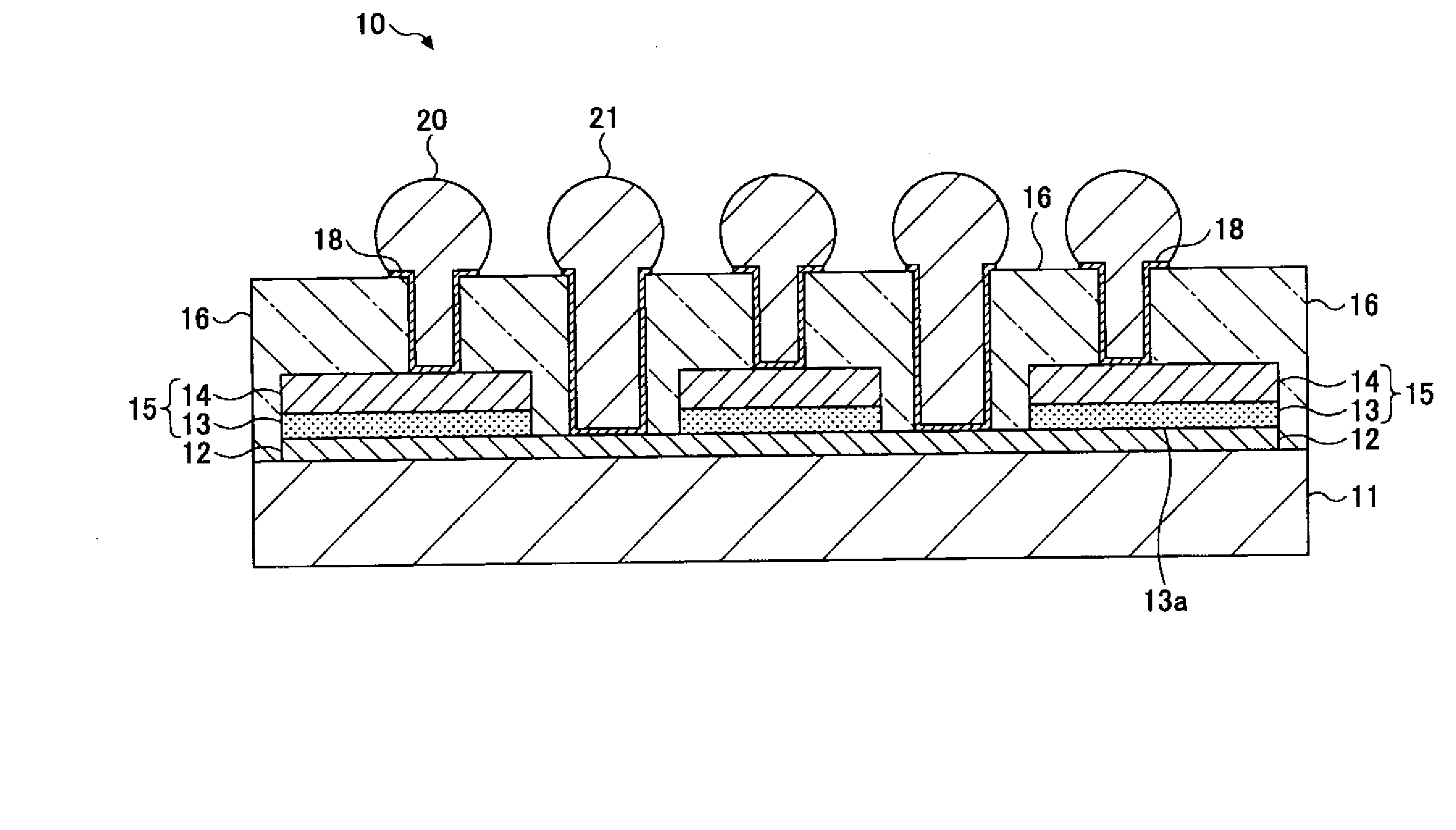
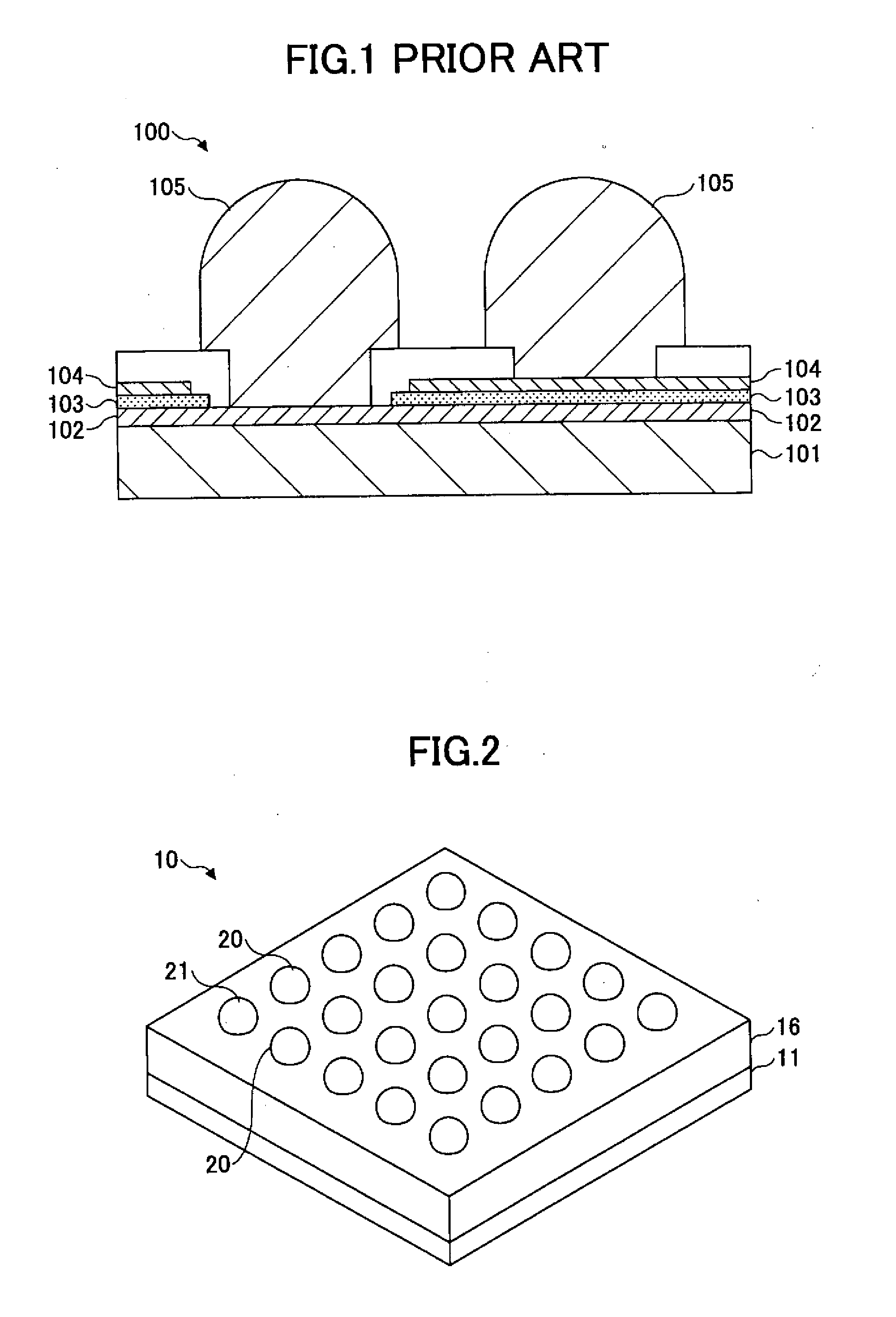
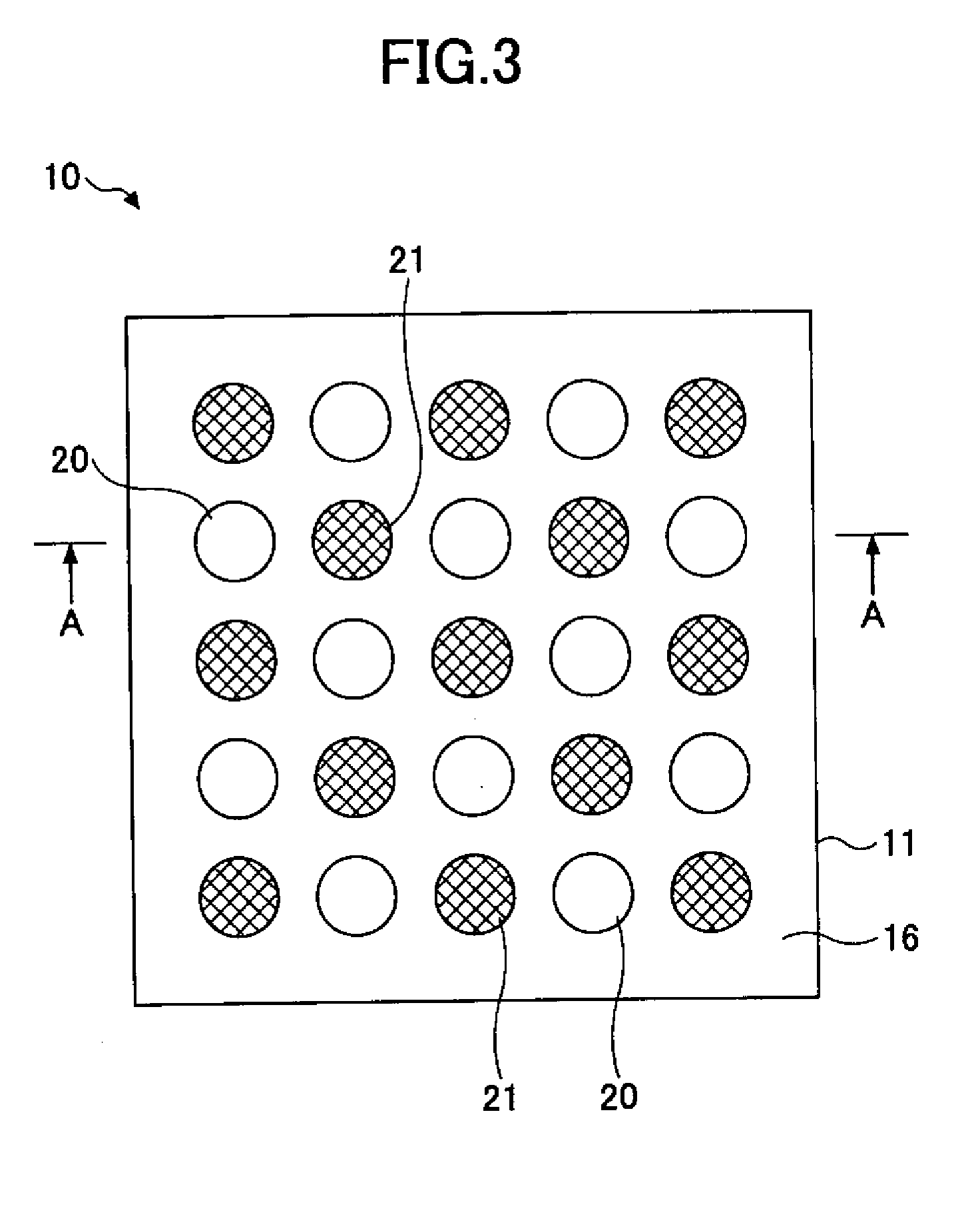
[0037]FIG. 2 is a perspective view of a capacitor in an embodiment of the invention. FIG. 3 is a plan view of the capacitor shown in FIG. 2. FIG. 4 is a cross-sectional view of the capacitor taken along the line A-A indicated in FIG. 3.

[0038] As shown in FIG. 2 through FIG. 4, the capacitor in this embodiment comprises a substrate 11, a lower electrode 12, a valve metal sheet 15, a protection layer 16, and electrode terminals 20, 21. The lower electrode 12 is formed on the substrate 11. The valve metal sheet 15 includes an oxide-film dielectric layer 13 formed on the lower electrode 12, and an upper electrode 14 formed on the dielectric layer 13. The protection layer 16 is provided so that the valve metal sheet 15 is enclosed in the protection layer 16. The electrode terminal 20 and the electrode terminal 21 are electrically connected to the upper electrode 14 and t...


PUM

PropertyMeasurementUnit
thicknessaaaaaaaaaa
thickaaaaaaaaaa
current densityaaaaaaaaaa

Abstract

A capacitor comprises a substrate, a conductive layer containing conductive particles, a valve metal sheet having a dielectric part formed throughout an entire surface of the conductive layer, a protection layer covering the valve metal sheet. The capacitor further includes a first electrode terminal electrically connected to the conductive layer and partially exposed from a surface of the protection layer, and a second electrode terminal electrically connected to a surface of the valve metal sheet opposite to a surface of the valve metal sheet on which the dielectric part is provided, and the second electrode terminal partially exposed from the surface of the protection layer. The dielectric part is made of an oxide of a metallic material of the valve metal sheet, the dielectric part is formed with a corrugated surface on the conductive layer, and the conductive particles are in contact with the corrugated surface.

Description

CROSS-REFERENCE TO RELATED APPLICATIONS [0001] This application is based upon and claims the benefit of priority of Japanese patent application No. 2006-254424, filed on Sep. 20, 2006, the entire contents of which are herein incorporated by reference. BACKGROUND OF THE INVENTION [0002] 1. Field of the Invention [0003] This invention generally relates to a capacitor, a manufacturing method thereof, and an electronic substrate including the capacitor, and more particularly to a capacitor which is appropriate for a decoupling capacitor, a manufacturing method of the capacitor, and an electronic substrate including the capacitor. [0004] 2. Description of the Related Art [0005] In recent years, in semiconductor integrated circuit devices including microprocessors, improvements for increased operating speed and reduced power consumption are advanced. In order to stabilize operation of a semiconductor integrated circuit device in high frequency areas in GHz bands, at low voltage, it is imp...

Claims


Application Information

Patent Timeline
Patent Type & Authority Applications(United States)
IPC IPC(8): H01G9/15H01G9/02H05K1/18
CPCH01G4/008H01G4/236H01G4/33H01L28/40Y10T29/43H05K1/181Y10T29/417Y10T29/435Y10T29/41H05K1/0231
Inventor SHIOGA, TAKESHIKURIHARA, KAZUAKI
Owner FUJITSU LTD
Learn More