Photoelectric conversion device and image capturing device
- Summary
- Abstract
- Description
- Claims
- Application Information
AI Technical Summary
Benefits of technology
Problems solved by technology
Method used
Image
Examples
first embodiment
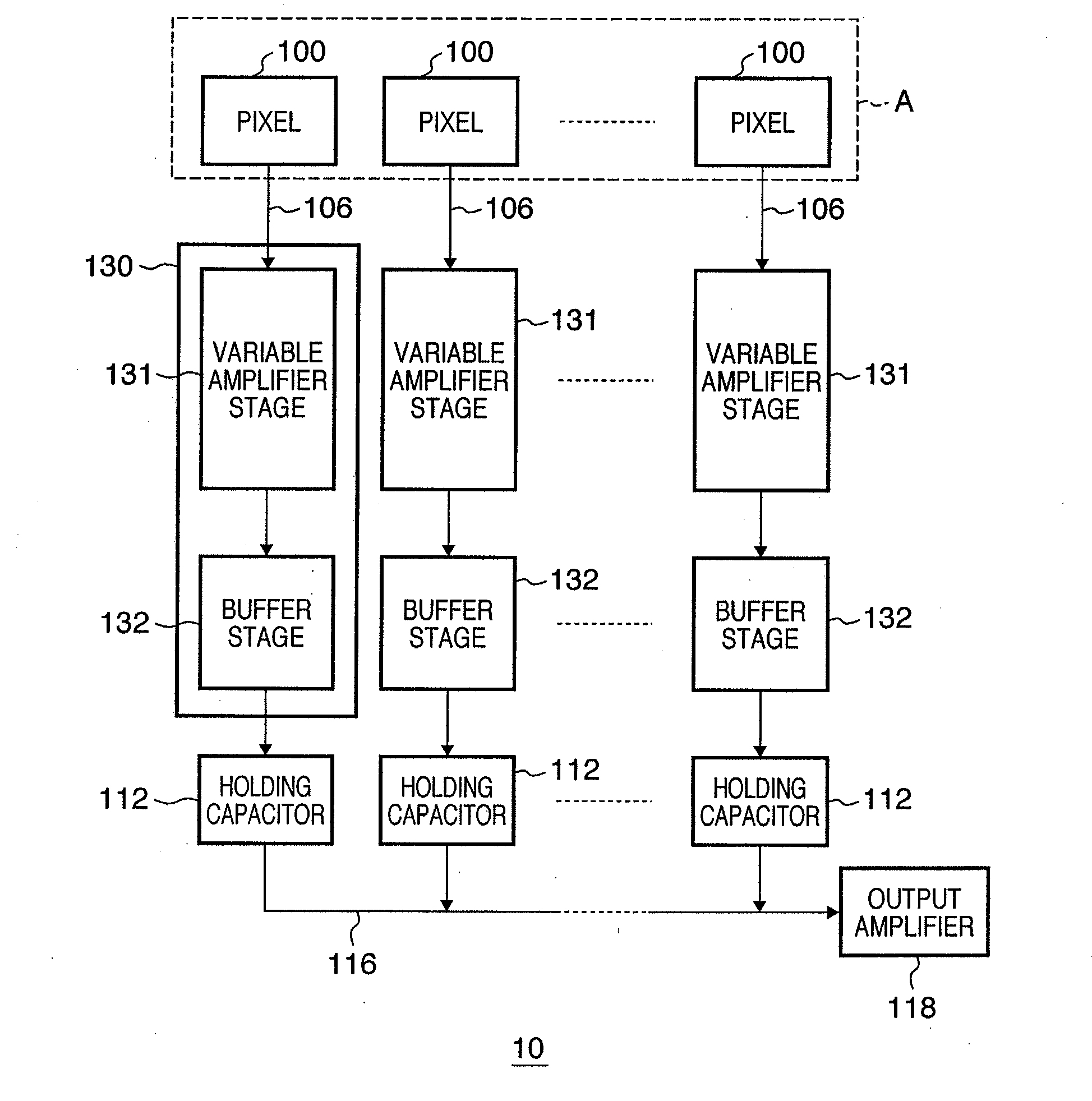
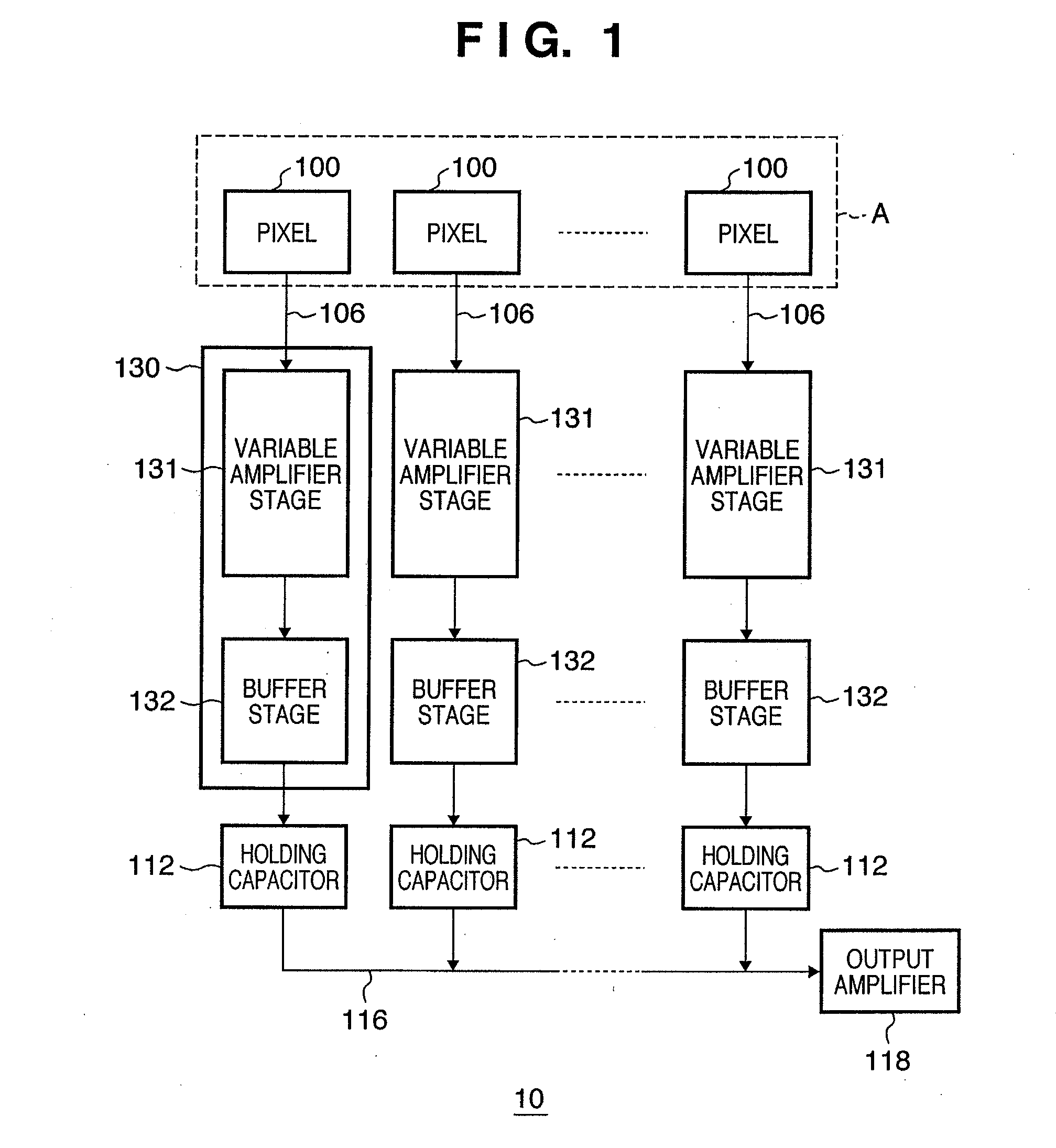
[0027]FIG. 1 is a block diagram showing the schematic arrangement of a photoelectric conversion device (solid-state image sensor) 10 according to the first embodiment of the present invention. Each pixel 100 includes a photoelectric converter such as a photodiode, and outputs a signal to a vertical output line (first pixel output line) 106 based on a signal obtained by photoelectrically converting incident light. Pixels 100 arrayed in a plurality of rows x a plurality of columns form pixel array A. A vertical scanning circuit (not shown) selects a row while a horizontal scanning circuit (not shown) selects a column. FIG. 1 shows pixels 100 arrayed in one row x a plurality of columns for descriptive convenience.
[0028]A column amplifier (amplifier unit) 130 receives a signal output to the vertical output line 106. The column amplifier 130 includes a variable amplifier stage 131, and a buffer stage 132 arranged on the output side of the variable amplifier stage 131. The variable amplif...
second embodiment
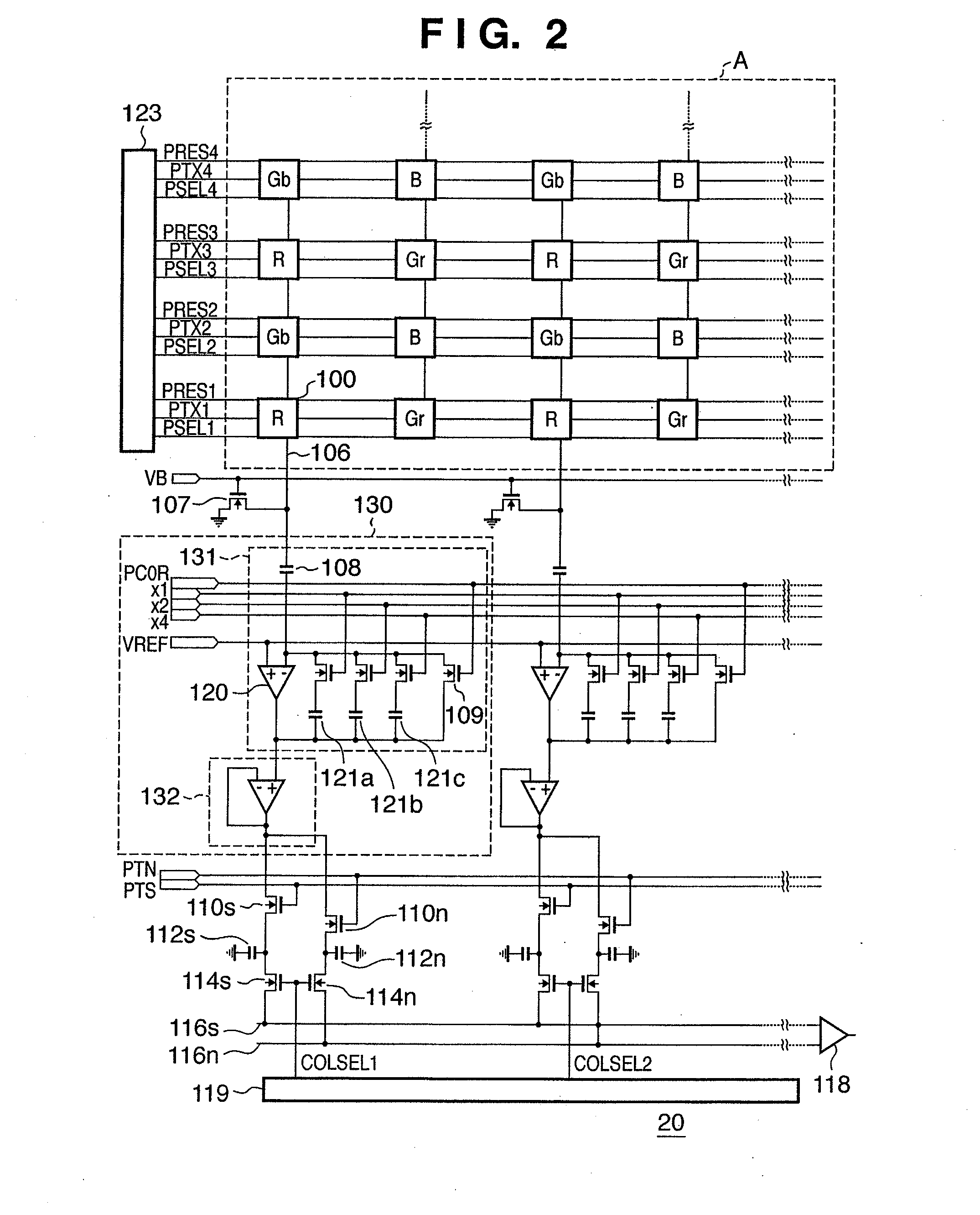
[0035]FIG. 2 is a circuit diagram showing the schematic arrangement of a photoelectric conversion device (solid-state image sensor) 20 according to the second embodiment of the present invention. Pixels 100 arrayed in a plurality of columns x a plurality of rows form pixel array A. Color filters R, Gr, Gb, and B in the Bayer array are formed on the pixels 100. In pixel array A, basic units each of 2×2 pixels are two-dimensionally arrayed.
[0036]A pixel having an R color filter will be called an R pixel; a pixel having a Gr color filter, a Gr pixel; a pixel having a Gb color filter, a Gb pixel; and a pixel having a B color filter, a B pixel.
[0037]Signals from R and Gb pixels are read out by a readout circuit arranged below pixel array A. Signals from B and Gr pixels are read out by a readout circuit (not shown) arranged above pixel array A.
[0038]FIG. 3 is an equivalent circuit diagram of one pixel 100. The transfer pulse PTX drives a transfer switch 102. The reset pulse PRES drives a ...
third embodiment
[0055]FIG. 6 is a circuit diagram showing the schematic arrangement of a photoelectric conversion device (solid-state image sensor) 30 according to the third embodiment of the present invention. The photoelectric conversion device 30 according to the third embodiment is different from the photoelectric conversion device 20 according to the second embodiment in that a buffer stage 132 in a column amplifier 130 is formed from a source follower.
[0056]As a feature of the photoelectric conversion device 30 according to the third embodiment, the number of elements which form the buffer stage 132 is small. As another feature, when a holding capacitor 112 is charged with a column amplifier output corresponding to the saturation light quantity, it is possible to charge the holding capacitor 112 regardless of the constant current value.
[0057]When a signal written in the holding capacitor increases in voltage along with an increase in light quantity, the source follower which forms the buffer ...
PUM
 Abstract
Description
Claims
Application Information
 - R&D
- Intellectual Property
- Life Sciences
- Materials
- Tech Scout
- Unparalleled Data Quality
- Higher Quality Content
- 60% Fewer Hallucinations
Browse by: Latest US Patents, China's latest patents, Technical Efficacy Thesaurus, Application Domain, Technology Topic, Popular Technical Reports.
© 2025 PatSnap. All rights reserved.Legal|Privacy policy|Modern Slavery Act Transparency Statement|Sitemap|About US| Contact US: help@patsnap.com


