
Data storage device and method

a data storage and data technology, applied in the field of data storage, can solve the problem of only adding a small marginal cos

Inactive Publication Date: 2007-11-15
INGENIA HLDG LTD
View PDF8 Cites 43 Cited by
  • Summary
  • Abstract
  • Description
  • Claims
  • Application Information

AI Technical Summary

Benefits of technology

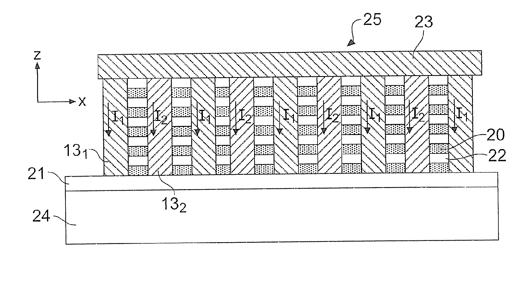
[0019] With this device, information can be moved down a magnetic nanowire by a combination of external magnetic fields and locally applied pulses of energy, such as heat energy. The scheme can be scaled almost indefinitely in the z (out of plane) direction, thus allowing very dense 3D networks of stored information to be realised. All data reading and writing activity can be performed with a single overlayer and with the base level of the CMOS (complementary metal oxide semiconductor) or other integrated circuit basis, so there is no need to make multilayered electrical connections to the different z stacked storage layers. Importantly, the multiple storage layers can all use the same mask or other lithography design, and so can be made by a single lithographic step; different layers are defined by a superlattice-like deposition, i.e. a layer of magnetic material is deposited followed by a layer of non-magnetic material as a spacer, followed by a further layer of magnetic material etc), all with a single lithographic exposure. These two points mean that the manufacturing cost does not scale with the number of layers; all that changes is the time taken for the deposition, which adds only a small marginal cost.

Problems solved by technology

These two points mean that the manufacturing cost does not scale with the number of layers; all that changes is the time taken for the deposition, which adds only a small marginal cost.

Method used


Image

  • Data storage device and method
  • Data storage device and method
  • Data storage device and method

Examples


Embodiment Construction

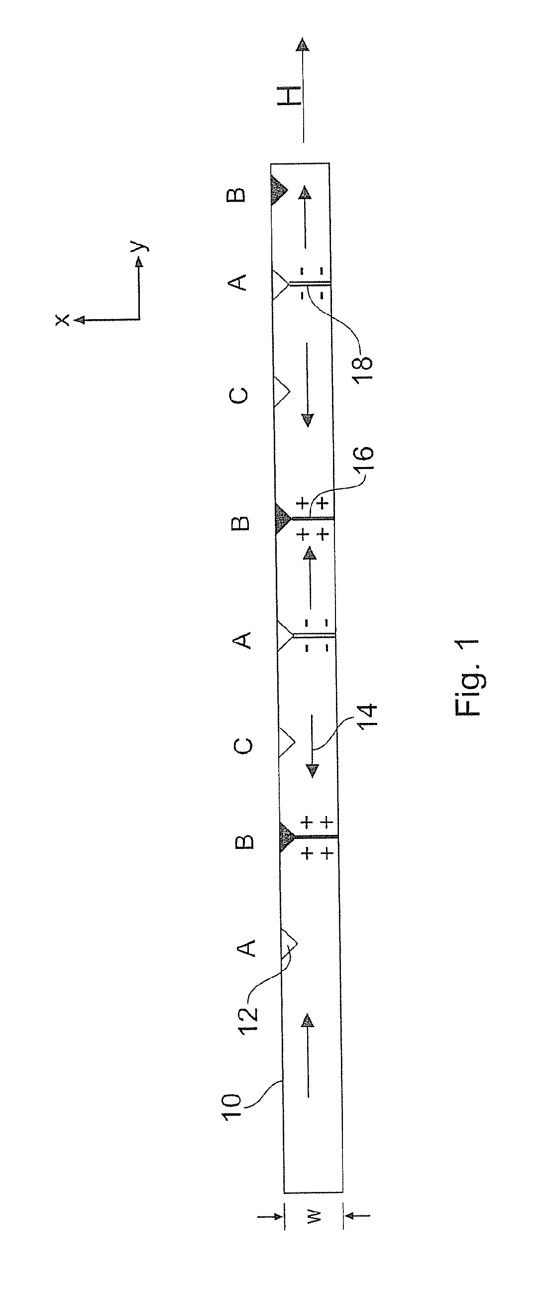
[0065]FIG. 1 is a schematic representation showing a portion of a nanowire 10 with a plurality of inward notches 12 along one side of the wire. The nanowire 10 is shown as being a relatively long, thin wire extending in a direction we define as the y-direction, not only in this figure but also in the following detailed description of an embodiment of the invention. The nanowire has a length ‘l’ (in the y-direction) longer than the illustrated portion and a width ‘w’ (in the x-direction). The nanowire width is typically in the submicron range, such as less than 0.2 μm (200 nm), more especially a width of the order of what is achievable with conventional lithography (currently 130 nm-65 nm but ever reducing). The nanowire will of course also have a depth ‘d’ in the z-direction defined by deposition of the nanowire. Typically, the nanowires will be fabricated by some form of deposition process, such as chemical vapour deposition (CVD), physical vapour deposition (PVD), thermal evaporat...


PUM


Abstract

A serial magnetic mass storage device and associated data storage method of the kind in which data is encoded in single magnetic domains in nanowires. In the invention, the nanowires are provided with a large number of notches along their length to form domain wall pinning sites. Moreover, the notches are addressed in groups (A, B, C) by heating electrodes. By alternately heating the notches hosting head-to-head and tail-to-tail domain walls in synchrony with alignment and anti-alignment of an operating field (H) along the nanowire the magnetic domains are moved along the nanowire by alternate movement of the head-to-head and tail-to-tail domain walls in caterpillar or worm-like motion in which the domains are incrementally lengthened and shortened by one inter-notch distance as they move along the nanowires under the joint coordinated action of the heating and alternating operating field. From an interconnect and fabrication standpoint, the scheme can be scaled almost without restriction out of the plane of the substrate to provide hundreds or thousands of stacked layers of nanowires, thus allowing very dense three-dimensional networks of stored information to be realised.

Description

RELATED APPLICATIONS [0001] This application claims priority to and incorporates by reference U.S. provisional application No. 60 / 746,839 filed on May 9, 2006.FIELD OF THE INVENTION [0002] The present invention relates to data storage, more especially but not exclusively to mass storage memory devices capable of storing GBytes of data, and of storing data at high densities. [0003] Hard drives with magnetic disks are the dominant technology for mass data storage and retrieval in personal computers (PCs). With current technology hard disk drives have storage capacities of up to around 100-200 GBytes, although smaller capacity miniature units are used in some devices, such as portable music players, video players and other portably multimedia devices which typically have drive capacities in the range 30-40 GBytes, or even smaller devices for digital cameras of sub-10 GBytes. The basic structure of a hard drive can trace its heritage back to a 19th century gramophone, in that it is fund...

Claims


Application Information

Patent Timeline
IPC IPC(8): H01L29/08H01L35/24H01L51/40H01L51/00
CPCB82Y10/00B82Y25/00H01F1/0072G11C11/14G11C19/0808G11C5/02Y10S977/933
Inventor COWBURN, RUSSELL PAULPETIT, DOROTHEEREAD, DANPETRACIC, OLEG
Owner INGENIA HLDG LTD
Learn More