Light-emitting resonant structure driving raman laser
a raman laser and resonant structure technology, applied in the direction of laser details, electric discharge tubes, electrical apparatus, etc., can solve the disadvantage of high-speed electrons
- Summary
- Abstract
- Description
- Claims
- Application Information
AI Technical Summary
Benefits of technology
Problems solved by technology
Method used
Image
Examples
first embodiment
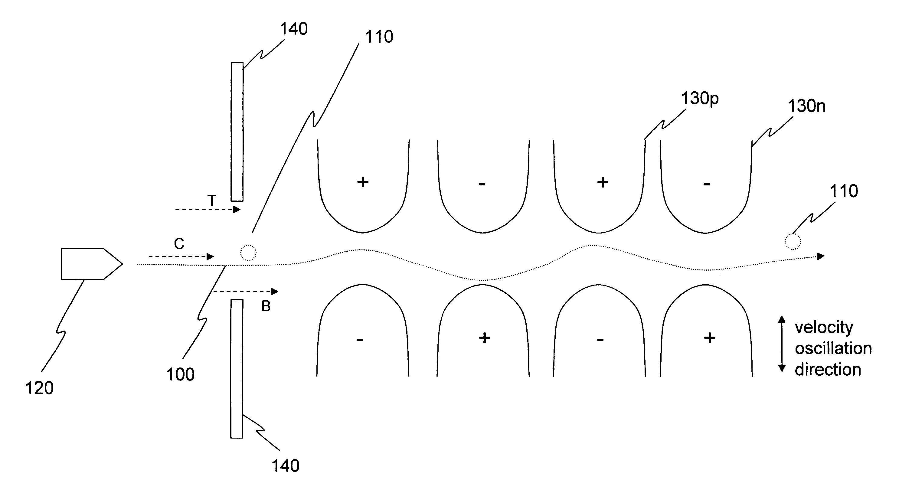
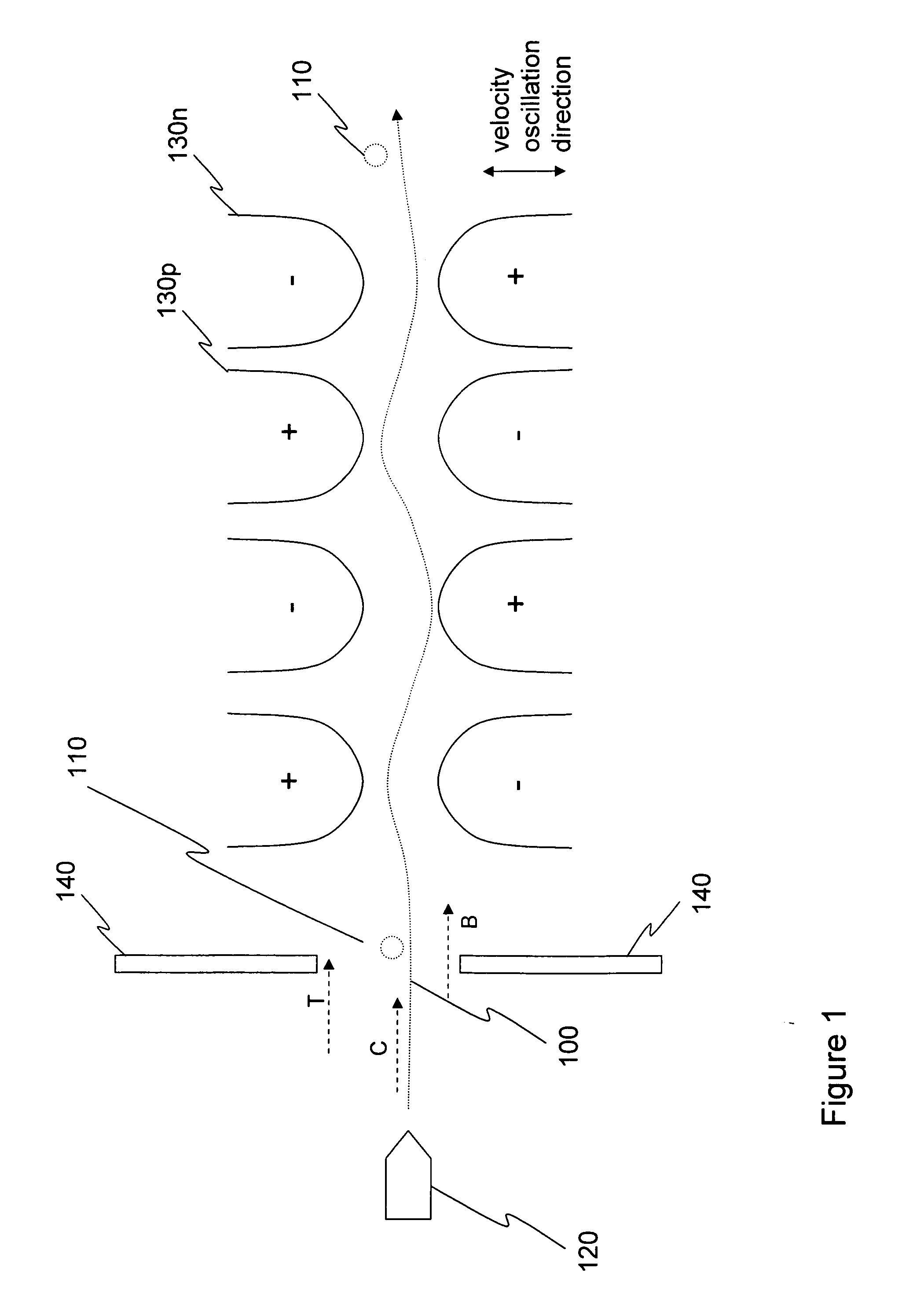
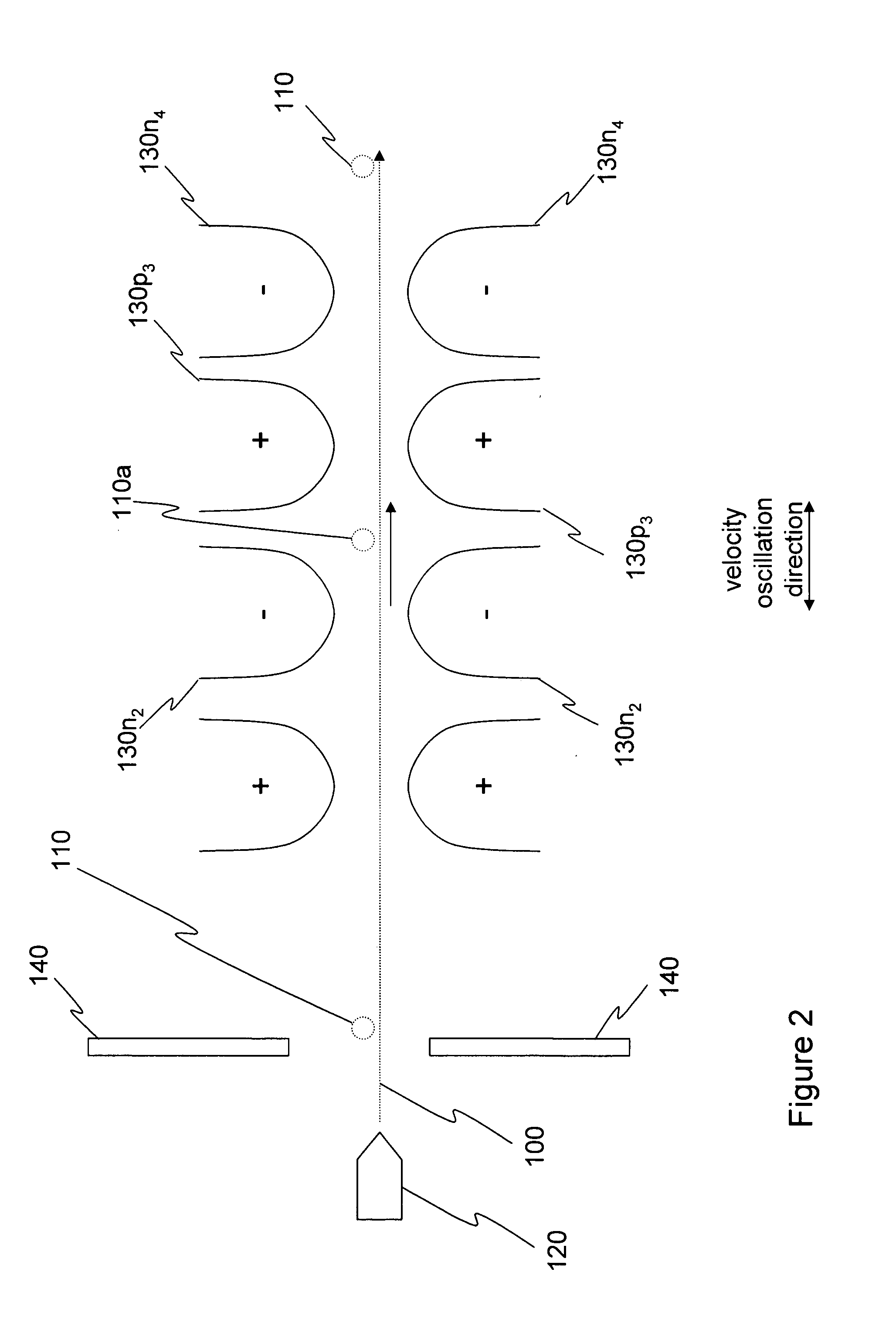
[0023] Turning now to the drawings, FIG. 1 is a high-level conceptual representation of a charged particle moving through a series of alternating electric fields according to the present invention. As shown therein, a charged particle beam 100 including charged particles 110 (e.g., electrons) is generated from a charged particle source 120. The charged particle beam 100 can include ions (positive or negative), electrons, protons and the like. The beam may be produced by any source, including, e.g., without limitation an ion gun, a thermionic filament, a tungsten filament, a cathode, a planar vacuum triode, an electron-impact ionizer, a laser ionizer, a chemical ionizer, a thermal ionizer, an ion-impact ionizer.
[0024] As the beam 100 is projected, it passes between plural alternating electric fields 130p and 130n. As used herein, the phrase “positive electric field”130p should be understood to mean an electric field with a more positive portion on the upper portion of the figure, and...
second embodiment
[0038] In light of the variation in paths that a charged particle can undergo based on its initial path between electrodes 140, in a coherent radiation source, a focusing element 700 is added in close proximity to the electrodes 140. The focusing element 700, while illustrated as being placed before the electrodes 140 may instead be placed after. In such a configuration, additional charged particles may traverse a center path between the fields and undergo constructive interference.
third embodiment
[0039] In a coherent light source, a pre-bunching element 800 is added which helps to control the inter-arrival time between charged particles, and therefore aid in the production of coherent Electromagnetic Radiation (EMR). One possible configuration of a pre-bunching element 800 is a resonant structure such as is described in U.S. application Ser. No. 11 / 410,924, [Attorney Docket No. 2549-0010] entitled “Selectable Frequency EMR Emitter,” filed on Apr. 26, 2006 and incorporated herein by reference. However, exemplary resonant structures are shown in FIGS. 9A-9H. As shown in FIG. 9A, a resonant structure 910 may comprise a series of fingers 915 which are separated by a spacing 920 measured as the beginning of one finger 915 to the beginning of an adjacent finger 915. The finger 915 has a thickness that takes up a portion of the spacing between fingers 915. The fingers also have a length 925 and a height (not shown). As illustrated, the fingers 915 of FIG. 9A are perpendicular to th...
PUM
 Abstract
Description
Claims
Application Information
 - R&D
- Intellectual Property
- Life Sciences
- Materials
- Tech Scout
- Unparalleled Data Quality
- Higher Quality Content
- 60% Fewer Hallucinations
Browse by: Latest US Patents, China's latest patents, Technical Efficacy Thesaurus, Application Domain, Technology Topic, Popular Technical Reports.
© 2025 PatSnap. All rights reserved.Legal|Privacy policy|Modern Slavery Act Transparency Statement|Sitemap|About US| Contact US: help@patsnap.com


