
Metal polishing slurry

a metal polishing and slurry technology, applied in the direction of lapping machines, manufacturing tools, other chemical processes, etc., can solve the problems of slowing affecting the polishing rate, so as to improve productivity, slow down the polishing rate, and improve the polishing rate

Inactive Publication Date: 2007-09-27
FUJIFILM CORP
View PDF15 Cites 15 Cited by
  • Summary
  • Abstract
  • Description
  • Claims
  • Application Information

AI Technical Summary

Benefits of technology

[0008]Recently, to improve productivity, wafer diameters during LSI fabrication have become larger, with diameters of 200 mm or more being currently the norm. LSI fabrication at wafer diameters of 300 mm or more has even begun. As the wafer size increases, differences in polishing rate tend to arise between the center and the edge of the wafer. Hence requirements for polishing uniformity across the wafer have become more and more exacting.
[0010]It is therefore an object of the present invention to provide a metal polishing slurry for use in chemical mechanical polishing (CMP) which is able to polish metals including copper at a high rate and causes minimal dishing.

Problems solved by technology

In polishing copper metal, because copper is a particularly soft metal, there is a tendency of certain undesirable phenomena to occur.
An example of a known process for chemically polishing copper and copper alloys, that is, a process which does not include a mechanical polishing means, is the method described in JP 49-122432 A. However, in contrast with CMP in which chemical and mechanical polishing is performed selectively on the metal film at raised features, due to the occurrence of dishing and the like at low features, planarity is a major challenge in chemical polishing processes that rely entirely on a chemical dissolving action.
Corrosion inhibitors such as benzotriazole are often used to keep excessive chemical dissolution from occurring, although this has had the undesirable effect of slowing the polishing rate.

Method used


Image

  • Metal polishing slurry
  • Metal polishing slurry
  • Metal polishing slurry

Examples


examples

[0106]Examples are given below by way of illustration and should not be construed as limiting the invention.

1. Preparation of Aluminum-Coated Colloidal Silica

[0107]Sodium hydroxide was added to 100 g of a 20 wt % aqueous dispersion of colloidal silica abrasive having an average particle size of 50 nm so as to adjust the pH to 9.5, following which 0.12 mmol of sodium aluminate was added at room temperature and the resulting mixture was stirred for 3 hours.

[0108]Assuming 100% reaction by the sodium aluminate added, the amount of silicon atoms on the surface of the colloidal silica that are substituted with aluminum atoms is 1% as represented as the colloidal silica surface atom substitution ratio (number of aluminum atoms introduced / number of surface silicon atom sites), based on the surface area calculated from the colloidal silica diameter, a specific gravity for colloidal silica of 2.2 and a number of silicon atoms per unit surface area of 13 / nm2.

[0109]Abrasive particles which were...


PUM

PropertyMeasurementUnit
particle sizeaaaaaaaaaa
pHaaaaaaaaaa
diametersaaaaaaaaaa

Abstract

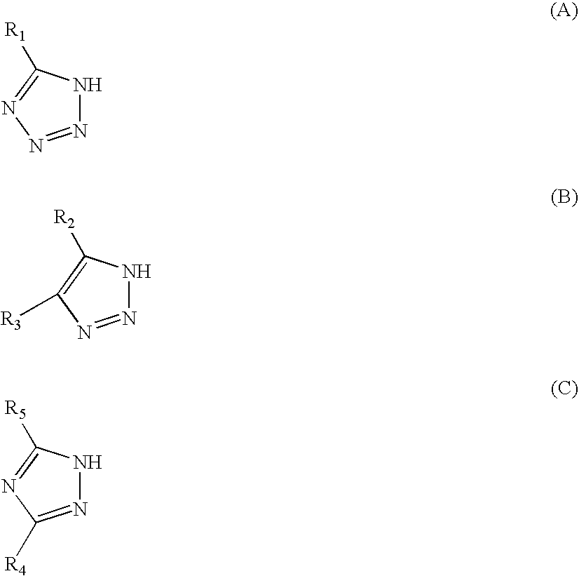
The metal polishing slurry according to the present invention for use in chemical mechanical polishing during semiconductor device fabrication contains at least one compound of formula (A) below and at least one compound of formula (B) or formula (C) below:[wherein R1, R2, R3, R4 and R5 are each independently hydrogen, methyl, ethyl, phenyl, amino, sulfo, carboxy, aminomethyl, carboxymethyl, sulfomethyl, o-aminophenyl, m-aminophenyl, p-aminophenyl, o-carboxyphenyl, m-carboxyphenyl, p-carboxyphenyl, o-sulfophenyl, m-sulfophenyl or p-sulfophenyl].

Description

[0001]The entire contents of all documents cited in this specification are incorporated herein by reference.BACKGROUND OF THE INVENTION[0002]The present invention relates to the manufacture of semiconductor devices. More particularly, the invention relates to a metal polishing slurry for use in the formation of interconnections in semiconductor devices, and to a polishing method which employs such a slurry.[0003]In the development of semiconductor devices such as semiconductor integrated circuits (referred to below as “LSI devices”), the trend toward smaller sizes and higher processing speeds has created a need in recent years for higher density and higher integration by the adoption of smaller design rules and multilayer constructions. Various techniques are being used to this end, including chemical mechanical polishing (CMP) wherein an insulating thin film (e.g., SiO2) and a metal thin film used to form interconnections are polished to planarize the substrate and remove surplus m...

Claims


Application Information

Patent Timeline
Patent Type & Authority Applications(United States)
IPC IPC(8): H01L21/4763B24B37/00C09K3/14H01L21/304
CPCC09G1/02C09K3/1463C09K3/1436H01L21/3212C09K3/14
Inventor YAMASHITA, KATSUHIRO
Owner FUJIFILM CORP
Learn More