Signal output circuit, communication apparatus and signal output control method
a communication apparatus and signal output technology, applied in the field of signal output circuits, communication apparatuses and signal output control methods, can solve the problems of high power consumption, complicated circuit configuration, loss of amplifier circuits, etc., and achieve the effect of reducing circuit power consumption and ensuring linearity
- Summary
- Abstract
- Description
- Claims
- Application Information
AI Technical Summary
Benefits of technology
Problems solved by technology
Method used
Image
Examples
first embodiment
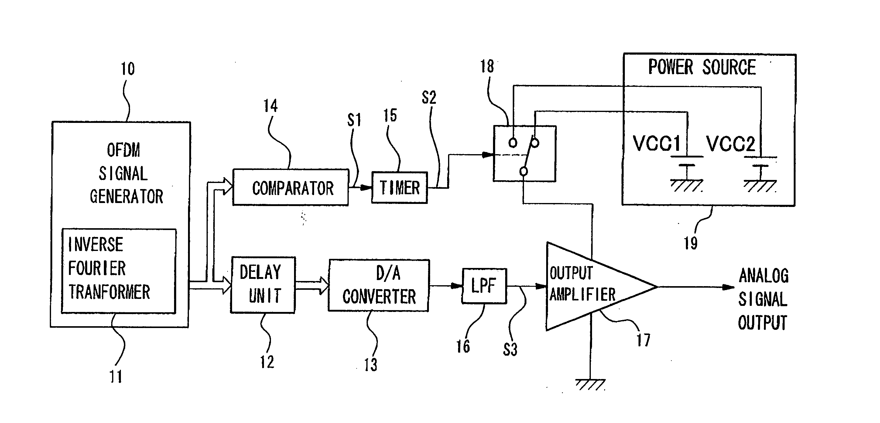
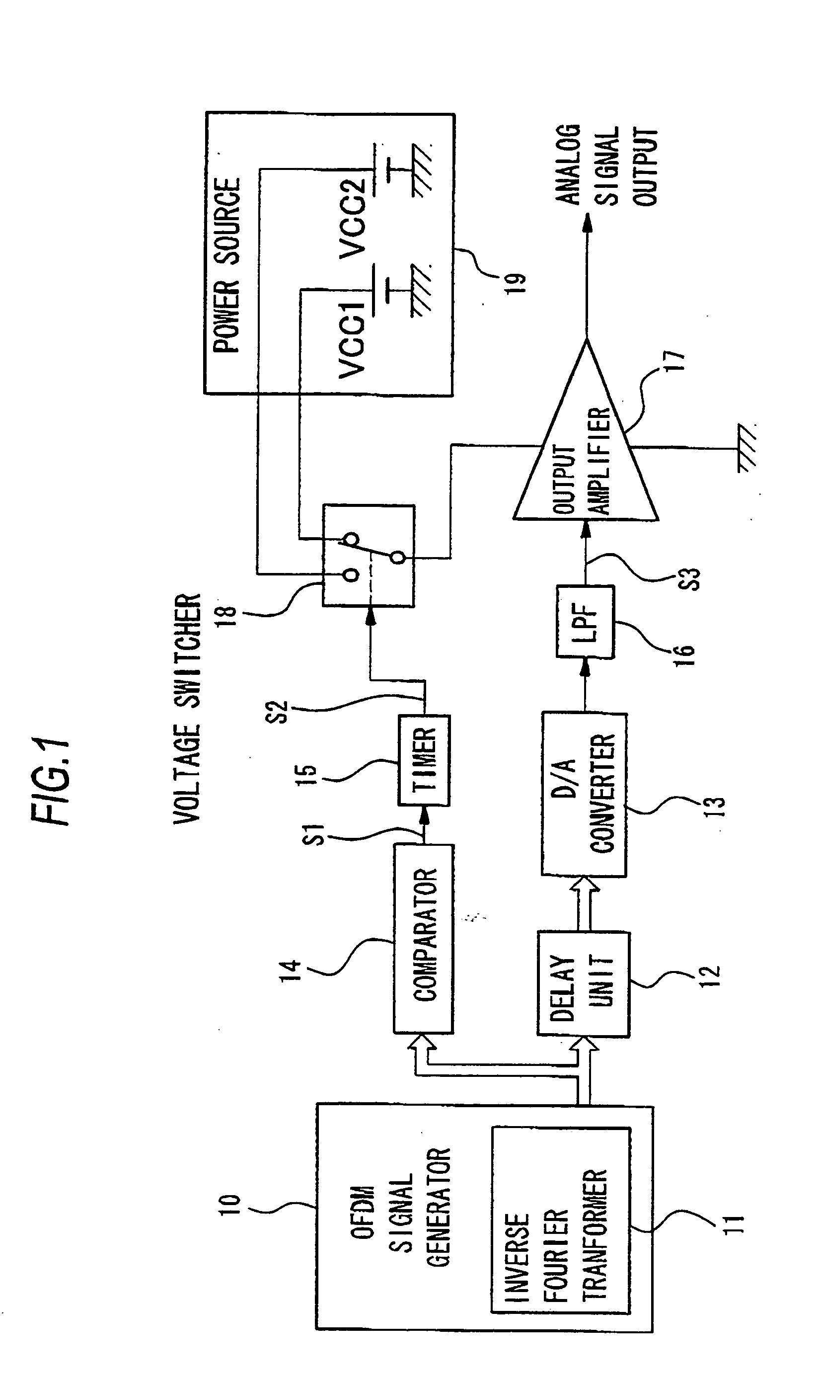
[0037] The OFDM signal output circuit described in the first embodiment, as shown in FIG. 1, includes: OFDM signal generator 10, which includes inverse Fourier transformer 11; delay unit 12; D / A converter 13; comparator 14; timer 15; LPF (low pass filter) 16; output amplifier17, which corresponds to an example of an output amplifier for performing signal amplification; voltage switcher 18, which switches power voltages; and power source 19.
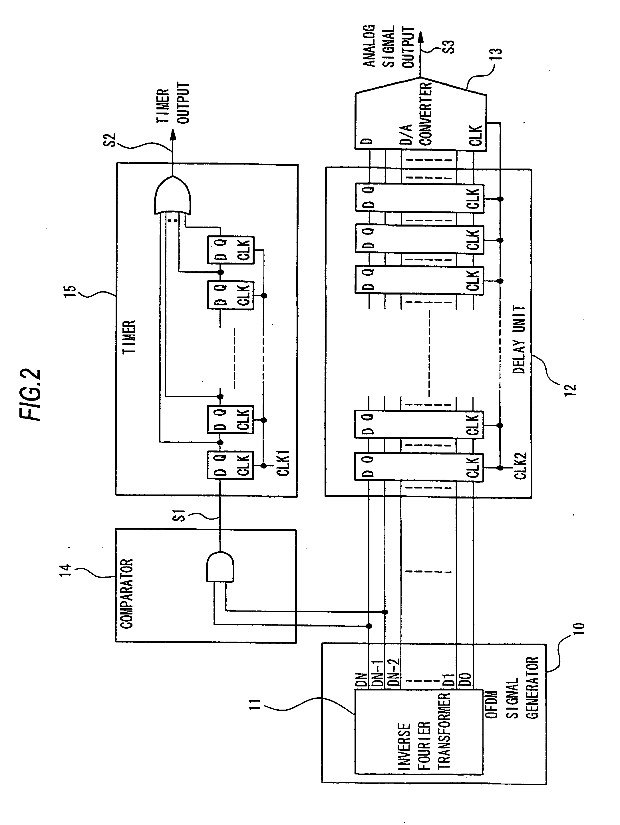
[0038] OFDM signal generator 10, which includes inverse Fourier transformer 11, generates time domain data containing amplitude information and phase information by performing inverse Fourier transform on frequency domain data, which are OFDM data generated through OFDM modulation. Such time domain data are supplied to delay unit 12 and comparator 14. Delay unit 12 delays time domain data for a predetermined period. Output data delayed by delay unit 12 are supplied to D / A converter 13 and converted into analog signals. Analog signals output from D...
second embodiment
[0049] The OFDM signal output circuit described in the second embodiment, as shown in FIG. 5, includes: OFDM signal generator 10 including inverse Fourier transformer 11; delay unit 12; D / A converter 13; comparator 24; timer 15; LPF (low pass filter) 16; output amplifier 27 that is operated by positive and negative power supplies; voltage switchers 28A and 28B that switch positive and negative power voltages, respectively; and power sources 29A and 29B that supply positive and negative power voltages, respectively.
[0050] Voltage switchers 28A and 28B have a function of switching positive and negative power voltages, which are supplied to output amplifier 27, in accordance with timer outputs from timer 15. While no timer output is being generated, voltage switcher 28A supplies, to output amplifier 27, positive low voltage power VCC3 from power source 29A; and voltage switcher 28B supplies, to output amplifier 27, negative low voltage power −VCC3 from power source 298. While a timer o...
third embodiment
[0057] The OFDM signal output circuit described in the third embodiment, as shown in FIG. 8, includes: OFDM signal generator 10 including inverse Fourier transformer 11; delay unit 12; D / A converter 13; comparator 14; timer 15; LPF (low pass filter) 16; output amplifier 17; power source 39; and intensifier (booster) 20.
[0058] Power source 39 includes only low voltage power supply VCC1. Intensifier (booster) 20 corresponds to an example of a power voltage controller. Intensifier (booster) 20 has a function of switching power voltages to be supplied to output amplifier 17, in accordance with timer outputs from timer 15. Intensifier (booster) 20 includes: diode 201 provided between the power terminal of output amplifier-17 and low voltage power supply VCC1; capacitor 202 connected at on end thereof to a connecting point (on a cathode side of diode 201) of the power terminal of output amplifier 17 and diode 201, the capacitor charging low voltage power VCC1, which is output from power s...
PUM
 Abstract
Description
Claims
Application Information
 - R&D
- Intellectual Property
- Life Sciences
- Materials
- Tech Scout
- Unparalleled Data Quality
- Higher Quality Content
- 60% Fewer Hallucinations
Browse by: Latest US Patents, China's latest patents, Technical Efficacy Thesaurus, Application Domain, Technology Topic, Popular Technical Reports.
© 2025 PatSnap. All rights reserved.Legal|Privacy policy|Modern Slavery Act Transparency Statement|Sitemap|About US| Contact US: help@patsnap.com


