
Redistribution connecting structure of solder balls

Active Publication Date: 2007-08-30
ADVANCED SEMICON ENG INC
View PDF8 Cites 42 Cited by
  • Summary
  • Abstract
  • Description
  • Claims
  • Application Information

AI Technical Summary

Benefits of technology

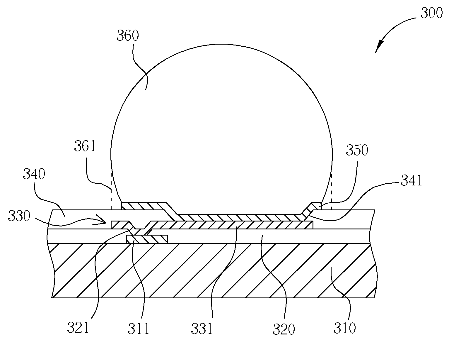
[0006]It is an objective of the present invention to provide a redistribution connecting structure to solve the aforementioned problem. According to the preferred embodiment of the present invention, a redistribution conductive layer is disposed between a first dielectric layer and a second dielectric layer on a substrate. The first dielectric layer partially exposes a plurality of bonding pads formed on the substrate, and the second dielectric layer partially exposes a plurality of redistribution pads formed on the redistribution conductive layer. Preferably, when a solder ball is disposed adjacent to a bonding pad having no electrical connection thereof and an opening of the first dielectric layer that exposes the bonding pad is covered by the surface of the solder ball, a substantially circular opening having a cut-off portion of the second dielectric layer is formed. Specifically, the opening of the second dielectric layer is formed adjacent to but not overlapping the opening of the first dielectric layer, thereby increasing the bonding area between the ball base and the redistribution pad and reducing the overall stress. Ultimately, phenomenon such as breaking or peeling of solder balls can be prevented, thus increasing the yield of the product.
[0007]According to an embodiment of the present invention, the redistribution connecting structure for solder balls includes a substrate, a first dielectric layer, a redistribution conductive layer, a second dielectric layer, at least a solder ball, and a first bonding pad and a second bonding pad disposed on the substrate. The first dielectric layer is disposed on the substrate, in which the first dielectric layer includes a first opening and a second opening partially exposing the first bonding pad and the second bonding pad. The redistribution conductive layer is formed on the first dielectric layer. The redistribution conductive layer includes a first redistribution pad and a second redistribution pad, in which the first redistribution pad is electrically connected to the first bonding pad through the first opening, and the second redistribution pad is electrically connected to the second bonding pad through the second opening. The second dielectric layer is formed on the first dielectric layer and the redistribution conductive layer. The second dielectric layer includes a third opening and a fourth opening, in which the third opening partially exposes the first redistribution pad and the fourth opening partially exposes the second redistribution pad. The solder ball is disposed on the first redistribution pad. The area of the solder ball preferably covers the third opening and a portion of the second opening. The third opening is substantially circular and disposed adjacent to but not overlapping the second opening, in which the third opening further includes a cut-off portion. By using this design, the solder ball can be disposed above the electrically insulated second bonding pad, thus reducing the overall stress and the eliminating the need for having additional redistribution conductive layers.

Problems solved by technology

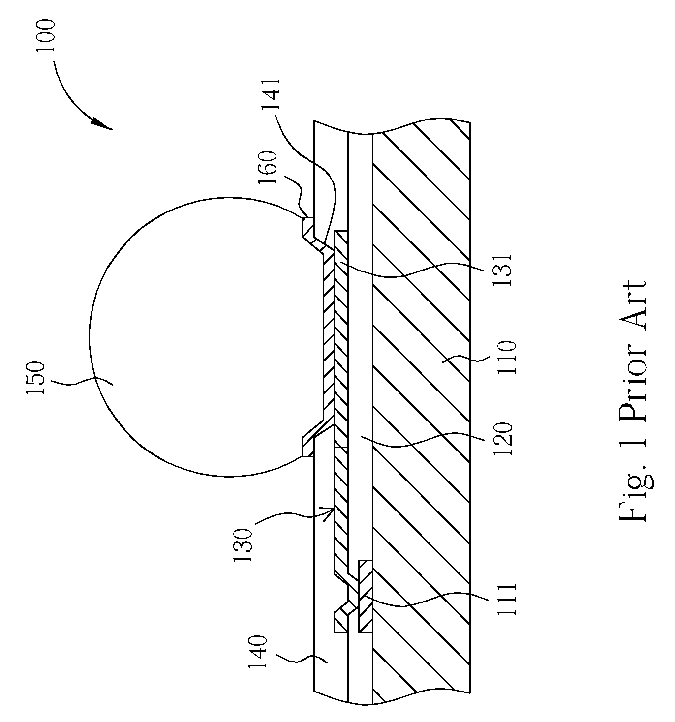
However, when the solder balls 150 are disposed too close to the bonding pads 111 having no electrical connection thereof, a stress will result and break the connection of the solder balls 150 and cause the solder balls to peel off.
This design ultimately limits the redistribution effect of the solder balls 150.

Method used


Image

  • Redistribution connecting structure of solder balls
  • Redistribution connecting structure of solder balls
  • Redistribution connecting structure of solder balls

Examples


Embodiment Construction

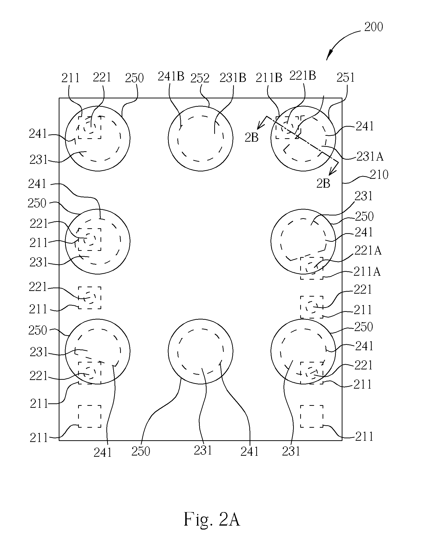
[0015]FIG. 2A illustrates a top-view of a redistribution connecting structure 200 for solder balls (i.e. solder bumps) according to the first embodiment of the present invention. FIG. 2B illustrates a cross-section of the redistribution connecting structure 200 of FIG. 2A along the sectional line 2B-2B.

[0016]As shown in FIGS. 2A and 2B, the redistribution connecting structure 200 includes a substrate 210 having a plurality of bonding pads 211, a first dielectric layer 220, a redistribution conductive layer 230, a second dielectric layer 240, and a plurality of the solder balls 250. The solder balls 250 include at least a first solder ball 251 and a second solder ball 252, and the bonding pads 211 include a first bonding pad 211A and a second bonding pad 211 B disposed on the substrate 210. The redistribution conductive layer 230 is used to electrically connect the first solder balls 251 and the first bonding pad 211A, and electrically connect the second solder ball 252 and the secon...


PUM


Abstract

A redistribution connecting structure for solder balls is disclosed. A substrate includes a plurality of bonding pads. A plurality of dielectric layers, a redistribution conductive layer between the dielectric layer, and a plurality of solder balls are formed on the substrate. The redistribution layer has a redistribution pad disposed adjacent to one of the bonding pads without electrical connection with the redistribution pad. One of the dielectric layers covering the redistribution conductive layer has an opening to partially expose the redistribution pad, in which the opening is approximately circular and has a cut-off portion so that the opening is adjacent to an opening of another of the dielectric layers exposing one of the bonding pads without overlapping. Accordingly, bonding area of the redistribution pad for a bonding pad under one of the solder balls can be expanded to reduce stress effect.

Description

BACKGROUND OF THE INVENTION[0001]1. Field of the Invention[0002]The invention relates to a technique involving the connection of solder balls (i.e. solder bumps) for electronic devices, and more particularly, to a redistribution connecting structure for solder balls.[0003]2. Description of the Prior Art[0004]In the conventional art, solder balls are commonly disposed on the output terminal of electronic devices for connecting to other external devices. As the demand for product miniaturization increases, the position of solder balls must be rearranged and adjusted accordingly. As shown in FIG. 1, a conventional redistribution connecting structure 100 includes a substrate 110, a first dielectric layer 120, a redistribution conductive layer 130, a second dielectric layer 140, and a plurality of solder balls 150. A plurality of bonding pads 111 is disposed on the substrate 110, in which only one bonding pad is illustrated in the figure. The first dielectric layer 120 is disposed on the...

Claims


Application Information

Patent Timeline
IPC IPC(8): H01L23/48
CPCH01L23/3114H01L23/525H01L2924/0002H01L24/13H01L2224/0401H01L2224/05572H01L2224/13027H01L2224/13022H01L2224/05556H01L24/10H01L2224/13099H01L2924/01013H01L2924/01022H01L2924/01029H01L2924/01079H01L2924/14H01L2924/01005H01L2924/01006H01L2924/01023H01L2924/01024H01L2924/01033H01L2924/014H01L2924/00012H01L2924/00H01L2224/05552H01L24/05H01L2224/023H01L2224/06051H01L2224/061H01L2224/13H01L2224/14104H01L2924/15787H01L2924/351H01L2924/0001
Inventor SU, YI-HSUAN
Owner ADVANCED SEMICON ENG INC
Learn More