
Driver for multi-voltage island/core architecture

a multi-voltage island and core architecture technology, applied in logic circuits, logic circuits, logic functions, etc., can solve the problems of static (leakage) power dissipation becoming a significant component of limiting the performance of integrated circuit chips, and high total chip power dissipation

Inactive Publication Date: 2007-08-16
GOOGLE LLC
View PDF1 Cites 0 Cited by
  • Summary
  • Abstract
  • Description
  • Claims
  • Application Information

AI Technical Summary

Benefits of technology

[0007] A system and method for providing a driver for a multi-voltage island/core architecture of an integrated circuit chip are provided. A complementary metal oxide semiconductor (CMOS) inverter is built with a high threshold voltage p-channel field-effect transistor (hi-Vt PFET) and a regular threshold voltage n-

Problems solved by technology

As complementary metal oxide semiconductor (CMOS) technologies are scaled, total chip power dissipation is becoming high and is limiting the performance of an integrated circuit chip.
Simultaneously, static (leakage) power dissipation is becoming a significant component of total chip power dissipation.
One problem is how to build a driver between two voltage islands / cores that have different Vdd.
However, a CMOS inverter also has the problem of leakage, i.e., subthreshold leakage current.
Raising threshold voltage of a CMOS inverter may reduce leakage and may increase noise margin, but may also result in serious loss in performance, for example, prolonged rise time.

Method used


Image

  • Driver for multi-voltage island/core architecture
  • Driver for multi-voltage island/core architecture

Examples


Embodiment Construction

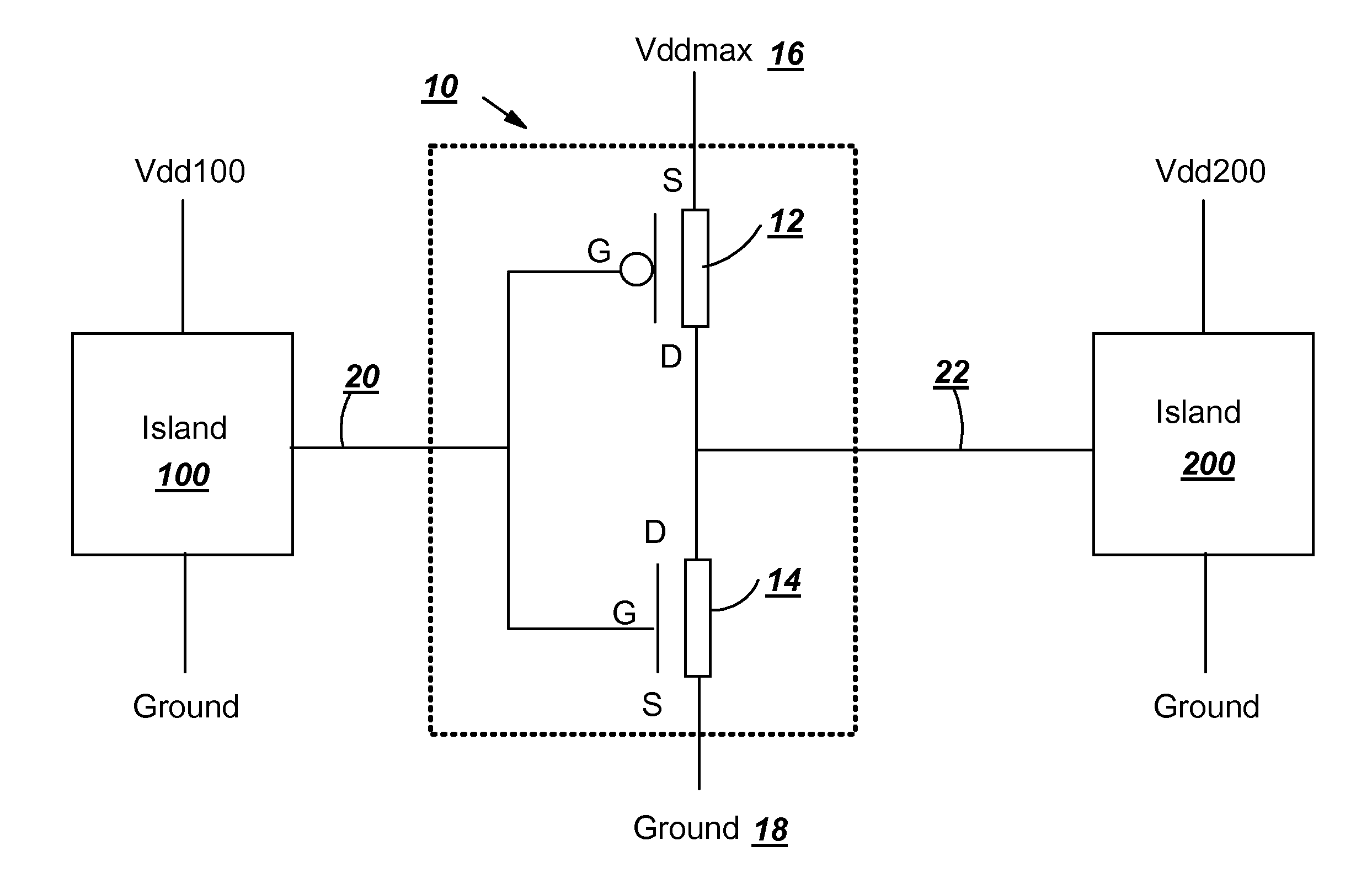
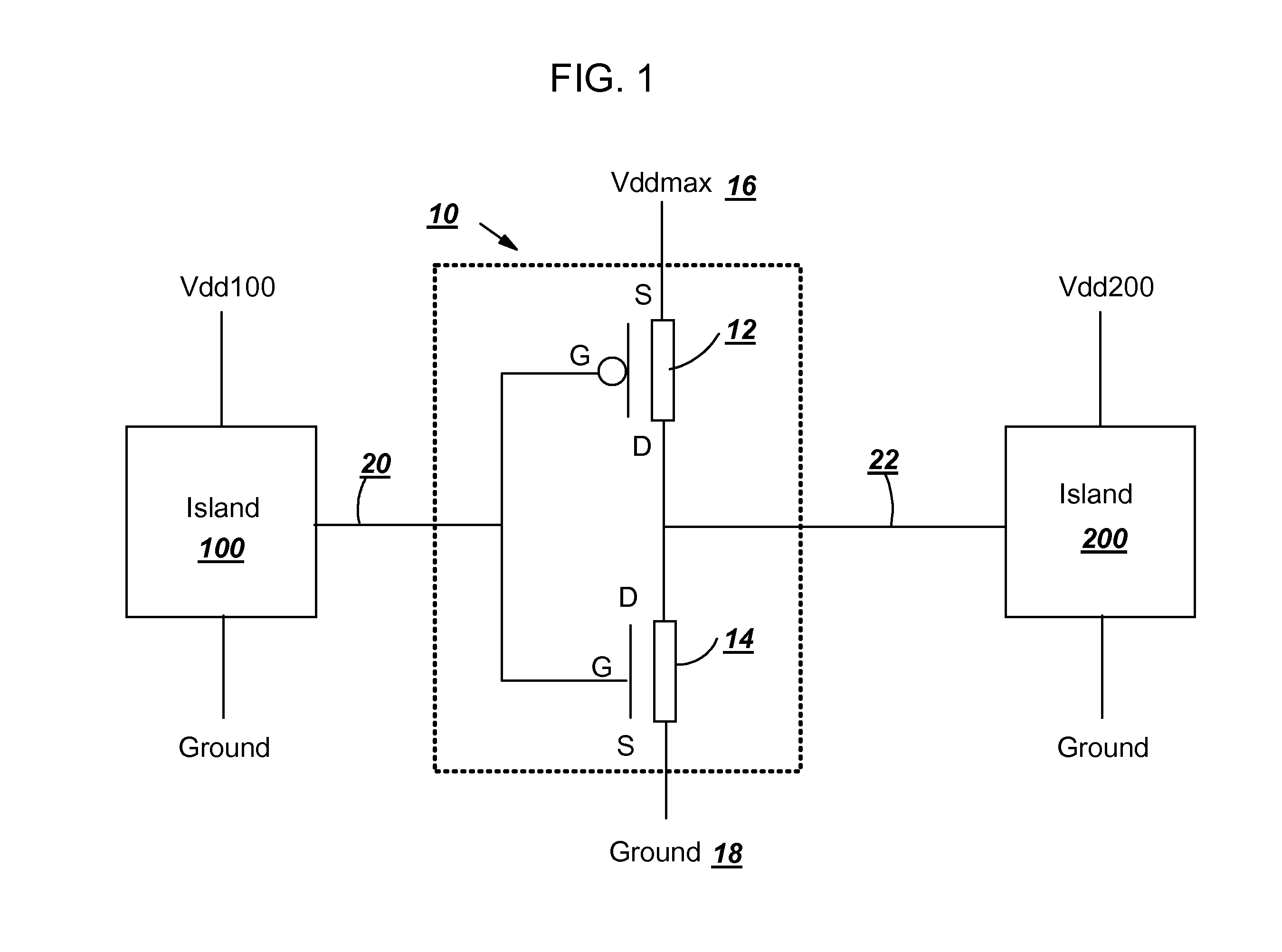
[0015] Turning to the drawings, FIG. 1 shows a block diagram of one embodiment of a driver 10 for a multi-voltage island / core of an integrated circuit (IC) chip (not shown). Driver 10 includes a high threshold voltage (hi-Vt) p-channel field-effect transistor (PFET) 12 and a regular threshold voltage n-channel field-effect transistor (NFET) 14, which are coupled together to form a complementary metal oxide semiconductor (CMOS) inverter. Specifically, source pin of hi-Vt PFET 12 is coupled to Vddmax 16, which is the maximum positive voltage supply (Vdd) on the IC chip; source pin of NFET 14 is coupled to chip ground 18; gate pins of hi-Vt PFET 12 and NFET 14 are coupled to form an input terminal 20 of driver 10; and drain pins of hi-Vt PFET 12 and NFET 14 are coupled to form an output terminal 22 of driver 10.

[0016] In FIG. 1, two voltage islands / cores (islands) 100 and 200 are coupled to driver 10 such that output of island 100 controls driver 10 to provide logic state to island 20...


PUM


Abstract

A system and method for providing a driver for a multi-voltage island / core architecture of an integrated circuit chip are provided. A complementary metal oxide semiconductor (CMOS) inverter is built with a high threshold voltage p-channel field-effect transistor (hi-Vt PFET) and a regular threshold voltage n-channel field-effect transistor (NFET), which uses the maximum positive voltage supply (Vdd) on the chip. The threshold voltage of the hi-Vt PFET is determined based on the maximum Vdd, the Vdd of the Voltage island / core that drives the CMOS inverter, and a subthreshold leakage current requirement of the hi-Vt PFET.

Description

BACKGROUND OF THE INVENTION [0001] 1. Technical Field [0002] The invention relates generally to multi-voltage island / core architectures, and more particularly, to a driver for a multi-voltage island / core architecture. [0003] 2. Background Art [0004] As complementary metal oxide semiconductor (CMOS) technologies are scaled, total chip power dissipation is becoming high and is limiting the performance of an integrated circuit chip. Simultaneously, static (leakage) power dissipation is becoming a significant component of total chip power dissipation. A multi-voltage island / core architecture is a solution to the power dissipations. A multi-voltage island / core architecture is designed to independently adjust the voltage supply (Vdd) of each function block in an integrated circuit chip so that the total and the static power dissipation is minimized for each function block while still meeting the chip performance requirements. Each function block with a voltage supply may be referred to as...

Claims


Application Information

Patent Timeline
IPC IPC(8): H03K19/0175
CPCH03K19/018521H03K19/0013
Inventor ANDERSON, BRENT A.BRYANT, ANDRESNOWAK, EDWARD J.
Owner GOOGLE LLC
Learn More