Semiconductor integrated circuit

a technology of integrated circuits and semiconductors, applied in the field of test circuits, can solve the problem of not being able to carry out burn-in tests that require sufficient stress on the memory, and achieve the effect of not reducing the memory access ra

Inactive Publication Date: 2007-08-02
RENESAS ELECTRONICS CORP
View PDF9 Cites 5 Cited by
  • Summary
  • Abstract
  • Description
  • Claims
  • Application Information

AI Technical Summary

Benefits of technology

[0020]According to the present invention, it is possible to provide a semiconductor device, which applies sufficient stress to the memory at the time of a burn-in test, without decreasing a memory access rate during normal operation.

Problems solved by technology

Therefore, it is not possible to carry out a burn-in test which requires application of sufficient stress to the memory.

Method used


Image

  • Semiconductor integrated circuit
  • Semiconductor integrated circuit
  • Semiconductor integrated circuit

Examples


Embodiment Construction

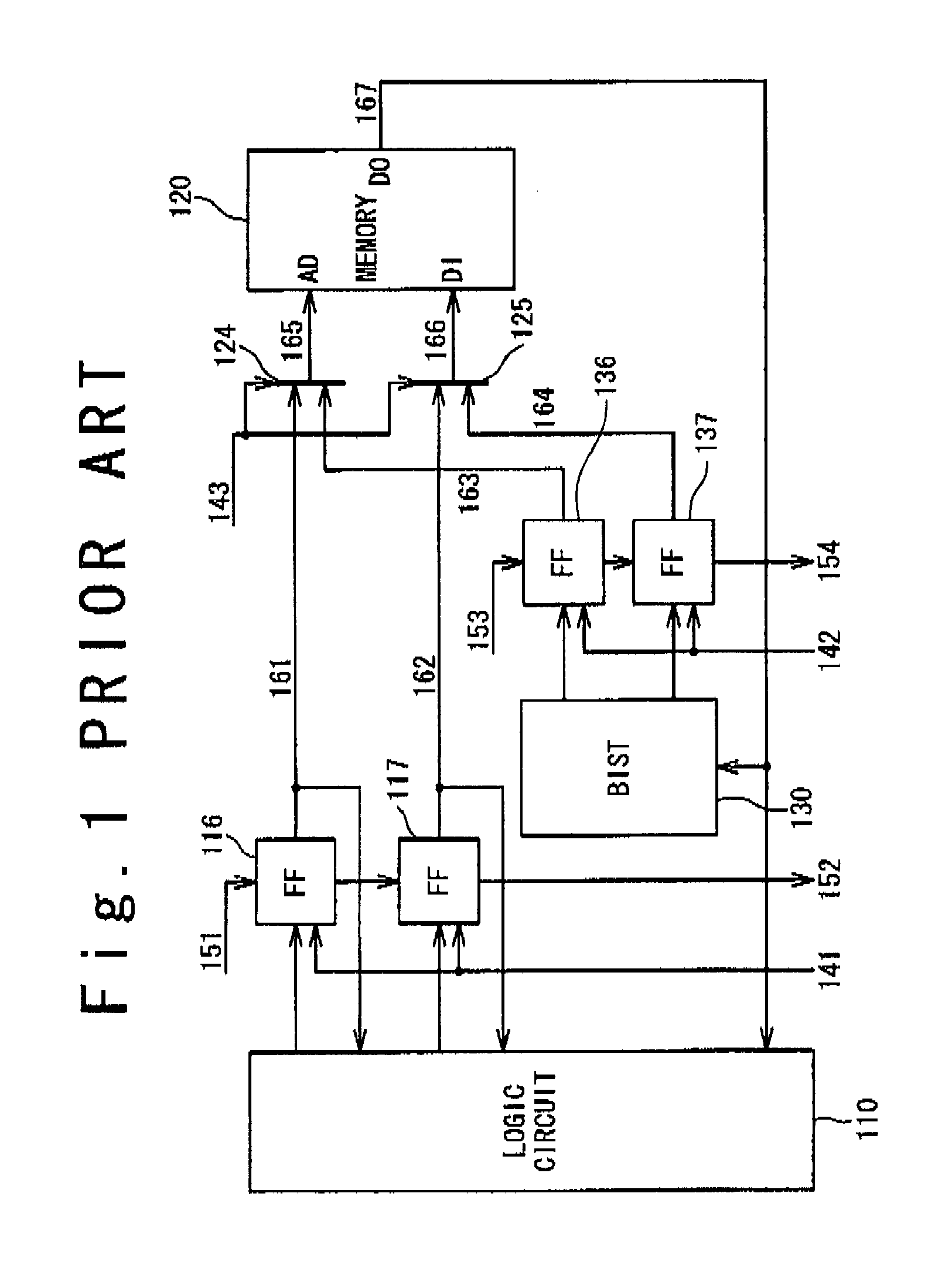
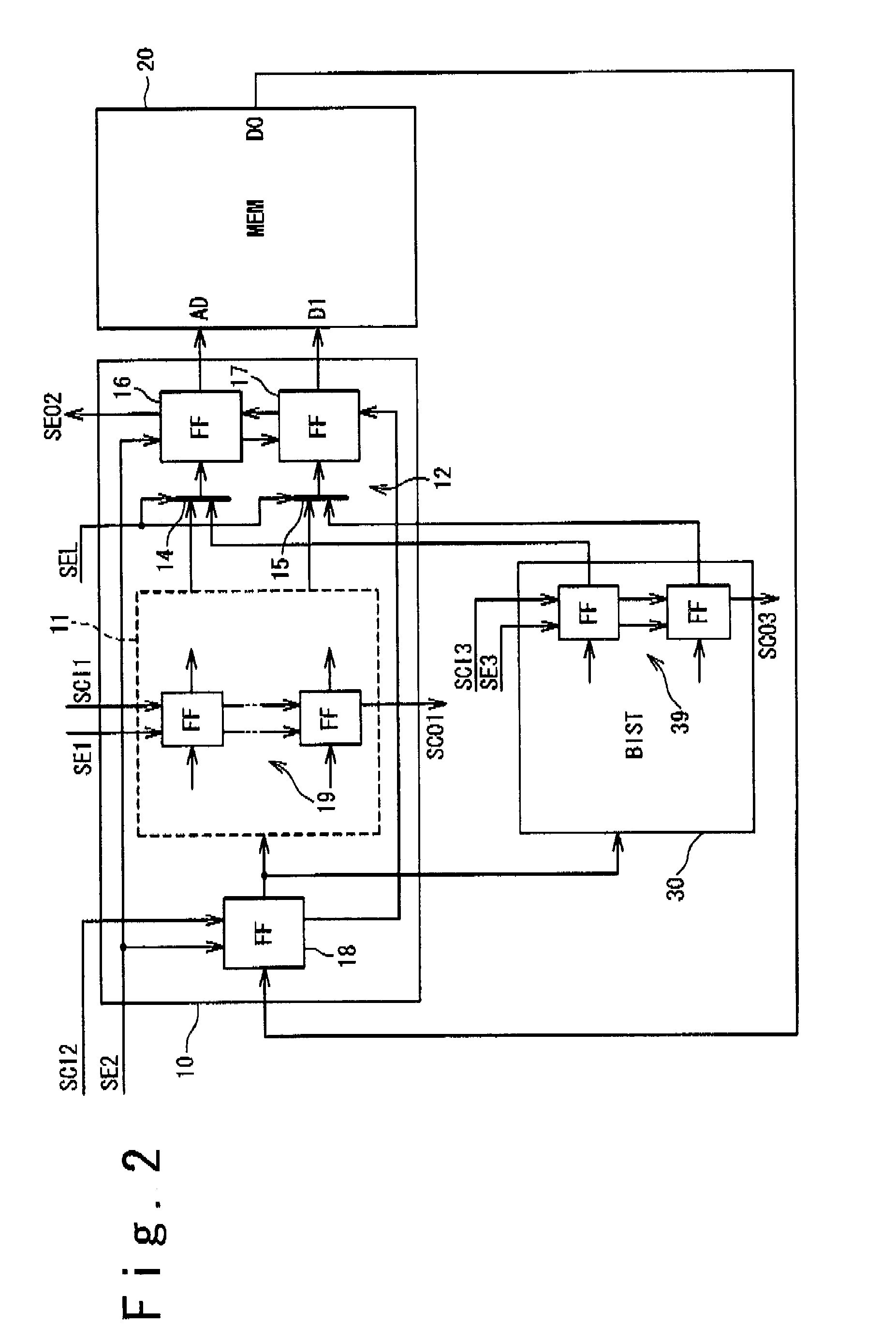
[0026]Hereinafter, a semiconductor integrated circuit of the present invention will be described with reference to the attached drawings. FIG. 2 is a block diagram showing the configuration of the semiconductor integrated circuit according to an embodiment of the present invention. The semiconductor integrated circuit includes a scan chain to test an internal logic and a BIST (Built-In Self-Test) circuit to test a memory.

[0027]The semiconductor integrated circuit includes a main circuit 10, a memory circuit 20 and a BIST circuit 30. The main circuit 10 and the memory circuit 20 are macro blocks. The main circuit 10 includes an internal logic circuit 11 and a memory interface circuit 12, and accesses the memory circuit 20. The BIST circuit 30 generates a test pattern to be supplied to the memory circuit 20, compares an output from the memory circuit 20 with an expected value, for a test of the memory circuit 20. The main circuit 10 and the BIST circuit 30 are target circuits of scan ...


PUM


Abstract

A semiconductor integrated circuit includes: a first circuit having a plurality of scan chains; a second circuit connected with input / output signals of the first circuit; and a third circuit connected with the second circuit through the first circuit. The plurality of scan chains comprises a first scan chain that contains flip-flops whose input / output signals are connected with the second circuit, and a second scan chain that does not contain any flip-flop whose input / output signal is connected with the second circuit. The flip-flops operate as a shift register at a scan path test, and when the third circuit exchanges signals with the second circuit through the flip-flops of the first scan chain, the second scan chain of the first circuit operates as a shift register.

Description

BACKGROUND OF THE INVENTION[0001]1. Field of the Invention[0002]The present invention relates to a semiconductor integrated circuit, and particularly to a test circuit of a semiconductor integrated circuit.[0003]2. Description of the Related Art[0004]In a test of a semiconductor integrated circuit, a stress application test is carried out to early detect generation of its initial failure so that defectives products are removed. A circuit for the stress application test is disclosed in Japanese Laid Open Patent Application (JP-P2003-121509A). In this conventional example, a burn-in circuit of the semiconductor integrated circuit has a logic circuit, one or more functional macros, and a built-in self-test circuit. The logic circuit includes a scan chain in an internal circuit. The built-in self-test circuit autonomously carries out a functional macro test provided for every functional macro. In the burn-in circuit of this semiconductor integrated circuit, the logic circuit carries out...

Claims


Application Information

Patent Timeline
Patent Type & Authority Applications(United States)
IPC IPC(8): G01R31/28
CPCG01R31/318577G11C2029/3202G11C29/48
Inventor HIDAKA, ITSUO
Owner RENESAS ELECTRONICS CORP
Why Eureka
Try Eureka