Light-emitting device and method for the production of light-emitting device

Inactive Publication Date: 2007-07-19
PANASONIC CORP
View PDF9 Cites 23 Cited by
  • Summary
  • Abstract
  • Description
  • Claims
  • Application Information

AI Technical Summary

Benefits of technology

[0016]The invention has been worked out in the light of the aforementioned circumstances. Therefore, an aim of the invention is to provide a light-emitting device having a reduced dispersion of thickness of light-emitting layer, a uniform emission distribution and an excellent durability.
[0018]In this arrangement, the light-projecting region of the light-emitting element is provided on a flat surface, making it possible to form a light-emitting layer to a uniform thickness. Thus, a light-emitting device having a uniform emission distribution and a prolonged life can be provided.
[0020]Moreover, the light-detecting element incorporated in the light-emitting device of the invention has a larger element region than the light-projecting region, making it assured that the light outputted from the light-emitting layer can be detected. Thus, the precision in the detection of quantity of light to be used in the correction of light can be enhanced. At the same time, the conversion of light to electric signal can be efficiently made.
[0022]Further, in the case where the light-detecting element is composed of a thin film transistor formed at the same step as the thin film transistor (TFT) constituting the driving circuit, the resulting light-detecting element is covered by a light-transmitting electrode disposed on the substrate side of the electroluminescent element with an interlayer insulating film interposed therebetween. This light-transmitting electrode acts as a gate electrode of TFT and also acts as a gate insulating film effectively depending on the thickness of the interlayer insulating film and the dielectric constant dependent on the properties of the interlayer insulating film. The potential at the anode (light-transmitting electrode) of the electroluminescent element which is a light-emitting element causes the application of an electric field to the channel. Thus, the gate-source voltage VGS causes the properties of the thin film transistor as a light-detecting element to be controlled. It is known that since this thin film transistor as a light-detecting element tends to show a great output fluctuation in the region where a photoelectric current flows, it is effective to measure the region where no electric current flows, i.e., OFF region. Therefore, by controlling the thickness of the interlayer insulating film which is a gate insulating film or the properties of the interlayer insulating film such that the potential at the anode of this electroluminescent element can act as a gate voltage of the thin film transistor as a light-detecting element, the detection of quantity of light can be made to a higher precision. In order that the potential at the anode might thus be applied effectively as a gate potential, an arrangement is more effectively made such that the anode of the electroluminescent element fully covers the channel region of the thin film transistor as a light-detecting element.

Problems solved by technology

Accordingly, when this production process is effected, it is difficult to avoid the rise of production cost.
However, the aforementioned level difference due to the presence of the light-detecting element 120 makes it difficult to form the interlayer insulating film 103 to a constant thickness.
When the emission distribution is uneven, the shape of light spots to be exposed are uneven, resulting in the dispersion of effective area (area contributing to development) of electrostatic latent image formed by exposure among the pixels.
This causes the occurrence of density unevenness that deteriorates image quality.
Thus, when the electroluminescent element 110 deteriorates, image density unevenness occurs, causing the deterioration of image quality.
Moreover, when the emission distribution (in-plane distribution) changes with time, the coefficient of correlation of light detected by the light-detecting element 120 with light actually outputted from the light-projecting region ALE changes, making it impossible to detect the quantity of light to a high precision.

Method used


Image

  • Light-emitting device and method for the production of light-emitting device
  • Light-emitting device and method for the production of light-emitting device
  • Light-emitting device and method for the production of light-emitting device

Examples


embodiments

[0118]Embodiments of implementation of the embodiment will be described in connection with the attached drawings.

[0119]Embodiments 1 and 2 will be described focusing on a light head employing a light-emitting device according to the invention.

[0120]In Embodiment 3, an example of image forming device having a light head employing the light-emitting device according to the invention incorporated therein will be described in detail.

[0121]In Embodiments 4 and 5, examples of the configuration of a light-detecting element will be described.

[0122]In Embodiment 6, a display device employing the light-emitting device according to the invention will be described.

[0123]In Embodiments 7 to 11, the configuration of a light-detecting element will be described in detail.

embodiment 1

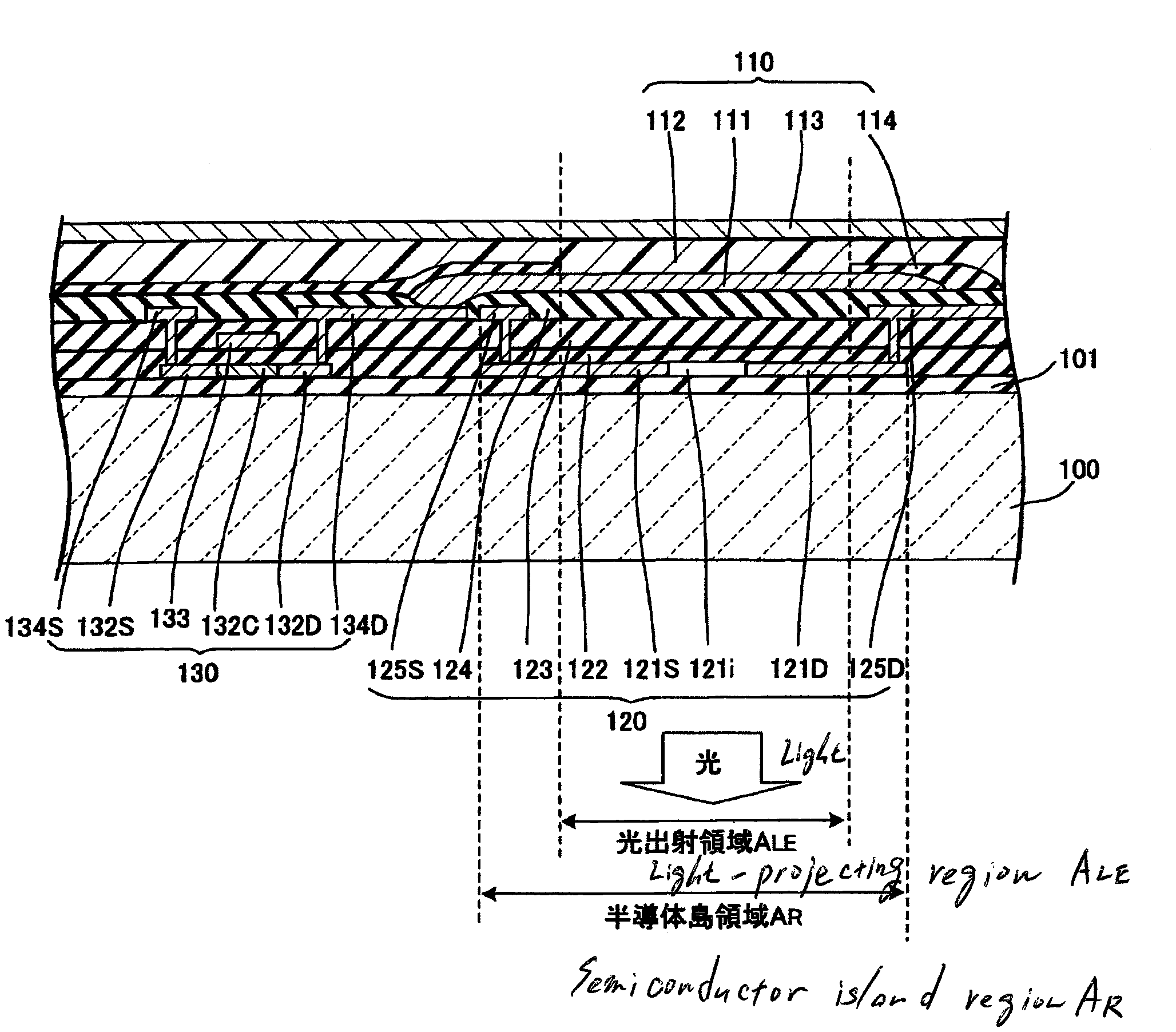
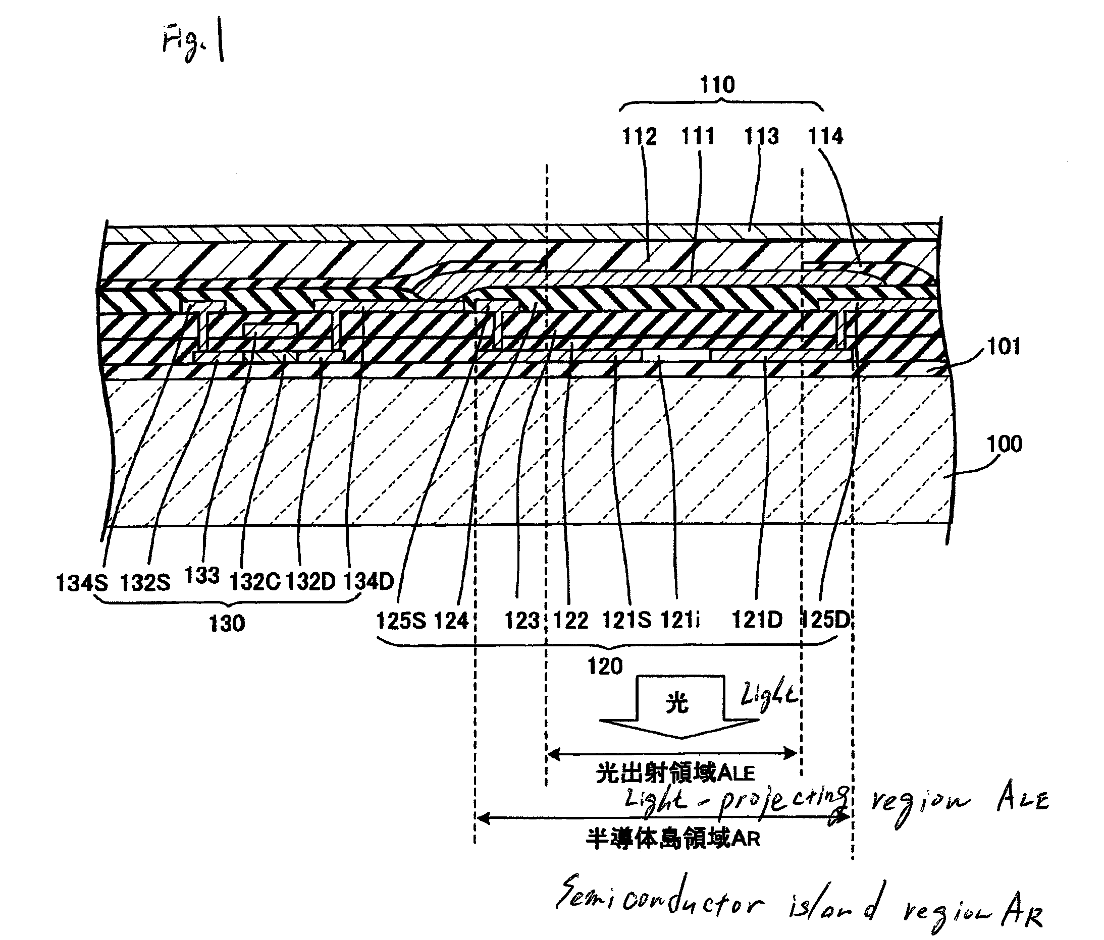
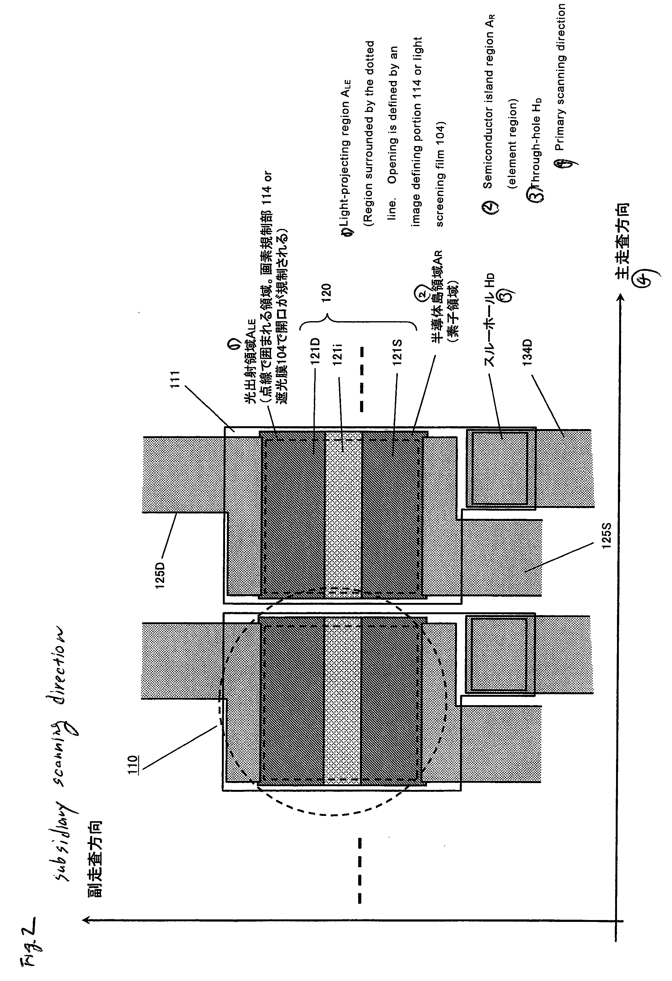
[0124]FIG. 1 is a sectional view illustrating the configuration of a light head employing the light-emitting device according to Embodiment 1, particularly the peripheral configuration of an electroluminescent element which is a light-emitting element provided in the light head. FIG. 2 is a plan view of the electroluminescent element according to Embodiment 1.

[0125]The disposition of the light-emitting element and light-detecting element according to the invention will be described in detail in connection with FIGS. 1 and 2.

[0126]FIG. 1 depicts the vertical positional relationship of the various layers constituting the electroluminescent element 110 which is a light-emitting element and the light-detecting element 120. In the light head, the electroluminescent element 110 is laminated on the top of a thin film transistor (TFT) constituting the light-detecting element 120 formed on the glass substrate 100 and the outer edge of a semiconductor island region made of a polycrystalline s...

embodiment 2

[0226]FIG. 7 is a sectional view of the light head according to Embodiment 2 in the form of top emission structure. The term “top emission structure” as used herein is meant to indicate a structure arranged such that the light outputted from the light-emitting layer 112 propagates toward cathodes 113a and 113b provided on the top of the light-emitting element 112 (surface of the glass substrate 100 having the thin film transistor and electroluminescent element 110 formed thereon) as opposed to the bottom emission structure.

[0227]In the configuration of FIG. 7, a reflective layer 105 made of a metal is provided on the glass substrate 100 so that the light is emitted in the direction toward the cathode. In FIG. 7, the reflective layer 105 is electrically connected to an electrode which is not shown or the like. By properly controlling the potential at the electrode, the light-detecting element 120 can be operated as a so-called bottom gate type transistor. In this manner, a light-emit...


PUM


Abstract

The invention concerns a light-emitting device comprising an electroluminescent element as a light source and a light-detecting element disposed superimposed on the electroluminescent element for detecting the quantity of light emitted by the electroluminescent element to generate an electric signal for use in the correction of the quantity of light emitted, wherein the light-detecting element has a semiconductor island region AR formed larger than a light-projecting region ALE and the thickness of the light-emitting layer in the light-projecting region ALE is uniform.

Description

BACKGROUND OF THE INVENTION[0001]1. Field of the Invention[0002]The present invention relates to a light-emitting device for use in display devices such as light head and display to be incorporated in image forming device and a method for the production thereof.[0003]2. Description of the Related Art[0004]In recent years, the reduction of size and cost of image forming devices such as facsimile and printer have been in rapid progress. Thus, the reduction of size and cost of elements constituting these devices is now under way.[0005]Examples of the method for forming an image using an image forming device include a heat-sensitive recording method which comprises making the use of the heat of a heat-generating element to cause heat transfer by which an image is formed, an ink jet method which comprises spreading a fine particulate ink over a printing material, and a method involving the use of light. Among these image forming devices, the image forming device which employs light allow...

Claims


Application Information

Patent Timeline
IPC IPC(8): H01L33/00
CPCH01L27/15H01L27/326H01L27/3269H01L31/022466H01L31/03682Y02E10/547H01L31/112H01L31/153H01L31/1804H01L31/202H01L31/03762Y02P70/50H10K59/121H10K59/13
Inventor HAMANO, TAKAFUMIYAMAMOTO, SHINYASHIROUZU, HIROSHI
Owner PANASONIC CORP
Why Eureka
Try Eureka