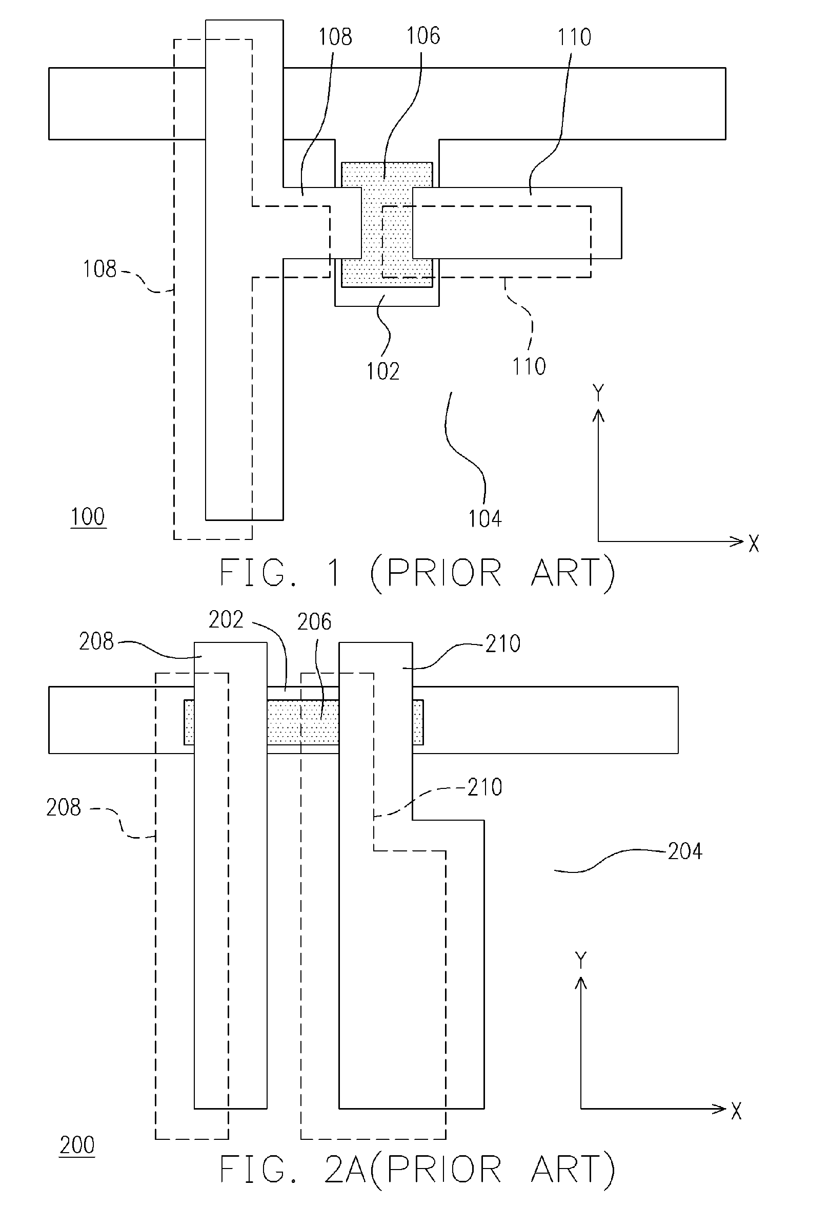
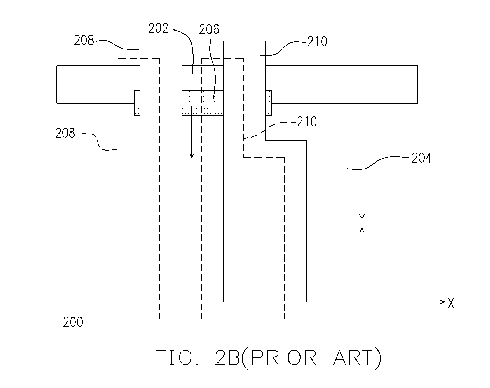
Thin film transistor
a thin film transistor and transistor technology, applied in the direction of basic electric elements, electrical equipment, semiconductor devices, etc., can solve the problems of large display size, occupying too much space, human eyes being hurt by the generated radiation, etc., and achieve the effect of significantly increasing the manufacturing yield
- Summary
- Abstract
- Description
- Claims
- Application Information
AI Technical Summary
Benefits of technology
Problems solved by technology
Method used
Image

Examples
first embodiment
The First Embodiment
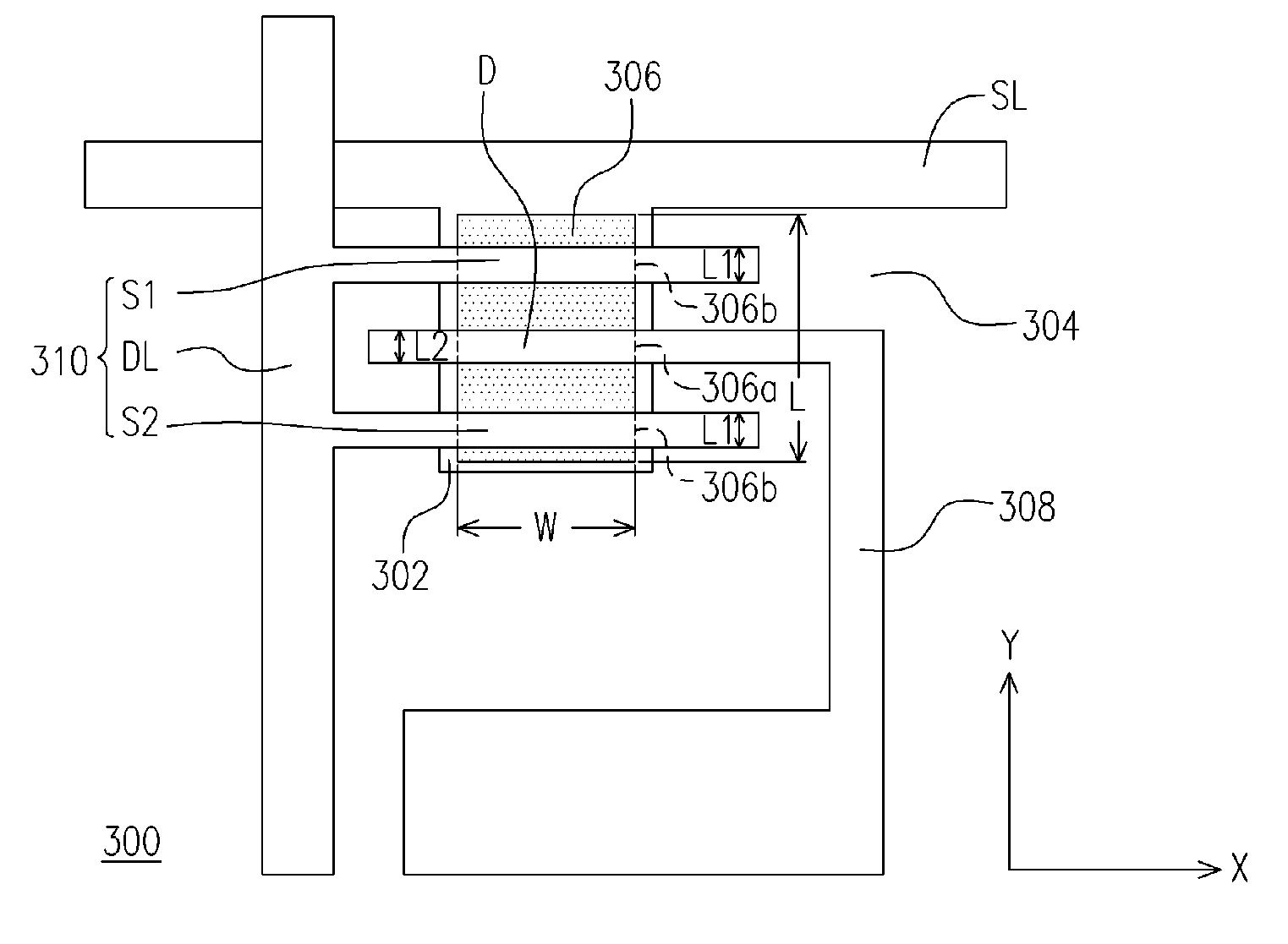
[0036]FIG. 3A is a schematic view of the layout of a thin film transistor according to a first embodiment of the present invention. Referring to FIG. 3A, a thin film transistor 300 of the present invention is suitable for being disposed on a flexible substrate (not shown). The thin film transistor 300 includes a gate 302, a gate insulating layer 304, a channel layer 306, a first conductive pattern 308, and a second conductive pattern 310. The gate 302 is disposed on the flexible substrate and the gate insulating layer 304 is disposed on the flexible substrate for covering the gate 302. The channel layer 306 is disposed on the gate insulating layer 304 and above the gate 302. The channel layer 306 has at least one first contact region 306a and multiple second contact regions 306b, and the first contact region 306a is located between the second contact regions 306b. In addition, the first conductive pattern 308 is disposed on a portion of the gate insulating layer ...
second embodiment
The Second Embodiment
[0043]FIG. 4A is a schematic view of the layout of a thin film transistor according to the second embodiment of the present invention. Referring to FIG. 4, a thin film transistor 300a of the present embodiment is similar to the thin film transistor 300 of the first embodiment. They are both the thin film transistor with dual source architecture. The mainly difference is that the extending direction of the source S1, source S2 and drain D. In particular, in the thin film transistor 300a of the present embodiment, the extending direction of the source S1, source S2 and drain D is in parallel with that of the data line DL.
[0044]FIG. 4B is a schematic view of a thin film transistor of the second embodiment, when misalignment occurs. Referring to FIG. 4B, when misalignments occur among the gate 302, the channel layer 306, the first conductive pattern 308, and the second conductive pattern 310 because of the expansion and the shrink of the flexible substrate resulted...
third embodiment
The Third Embodiment
[0045]FIG. 5A is a schematic view of the layout of a thin film transistor according to the third embodiment of the present invention. Referring to FIG. 5A, the thin film transistor 300b of the present embodiment is similar to the thin film transistor 300a of the second embodiment. The mainly difference is that the thin film transistor 300b of the present embodiment does not have the source S1, and only the source S2 and the data line DL are included. In particular, in the thin film transistor 300b of the present embodiment, the second conductive pattern 310 includes a source S2 and a data line DL connected to the source S2. The source S2 and the data line DL respectively cover the corresponding second contact regions 306b.
[0046] In the present embodiment, the extending direction of the source S2 and the drain D is parallel to that of the data line DL. In addition, the distributing position and the number of second contact regions 306b of the present embodiment d...
PUM
 Abstract
Description
Claims
Application Information
 - R&D
- Intellectual Property
- Life Sciences
- Materials
- Tech Scout
- Unparalleled Data Quality
- Higher Quality Content
- 60% Fewer Hallucinations
Browse by: Latest US Patents, China's latest patents, Technical Efficacy Thesaurus, Application Domain, Technology Topic, Popular Technical Reports.
© 2025 PatSnap. All rights reserved.Legal|Privacy policy|Modern Slavery Act Transparency Statement|Sitemap|About US| Contact US: help@patsnap.com