
Memory module comprising a plurality of memory devices

a memory module and memory device technology, applied in the field of memory modules, can solve the problems of inability to ensure the so-called “integrity” of data, and inability to achieve error correction in the event of failure of an entire devi

Inactive Publication Date: 2007-06-28
POLARIS INNOVATIONS
View PDF4 Cites 15 Cited by
  • Summary
  • Abstract
  • Description
  • Claims
  • Application Information

AI Technical Summary

Benefits of technology

[0027] Various aspects of the present invention ...

Problems solved by technology

Bit errors can occur both during the transfer of the data between module and controller and during the storage of the data in the module, with the result that the so-called “integrity” of the data is not always ensured.
This has the disadvantage, however, that in the event of failure of an entire device, a check bit always fails as well.
Consequently, the abovementioned technique which permits error correction in the event of failure of an entire device is made significantly more difficult or even becomes impossible.
Furthermore, ×9 devices are not advantageous if they are also intended to be used for forming a module for data operation without ECC.
If this stock consists of ×9 devices and if a non-ECC module is intended to be equipped therewith, then memory space is wasted.
For the same reasons, it is not only desirable but practically essential for the number L to be an integral power ≧2 of 2 (that is to say L=4, 8, . . . ), since ×1 and ×2 devices do not correspond to the conventional memory technology, that is to say are not customary commercially and would also be disadvantageous owing to the low data throughput.
In order to provide a two-core line for each bit stream in the bus, the number of conductor tracks in the bus could be doubled, but this is often undesirable, inter alia for space reasons.
This has the consequence, however, that the additional check bit memory device in the rank has only half as many bits to store as each useful bit memory device.
If all the devices are intended to be identical to one another, which is expedient for the reasons mentioned above, then the available total storage capacity of the module is not completely utilized, which is uneconomic.
Although this disadvantage could be eliminated by using a memory device having half the capacity (“half-dense memory device”) for check bit storage in each rank, said memory device is often not readily available or else belongs to an older technology generation, the products of which cannot readily be combined with the current generation (e.g. for reasons of the supply voltage).
However, this would result in the disadvantages as have been described further above in conjunction with the ×9 configuration.

Method used


Image

  • Memory module comprising a plurality of memory devices
  • Memory module comprising a plurality of memory devices
  • Memory module comprising a plurality of memory devices

Examples


Embodiment Construction

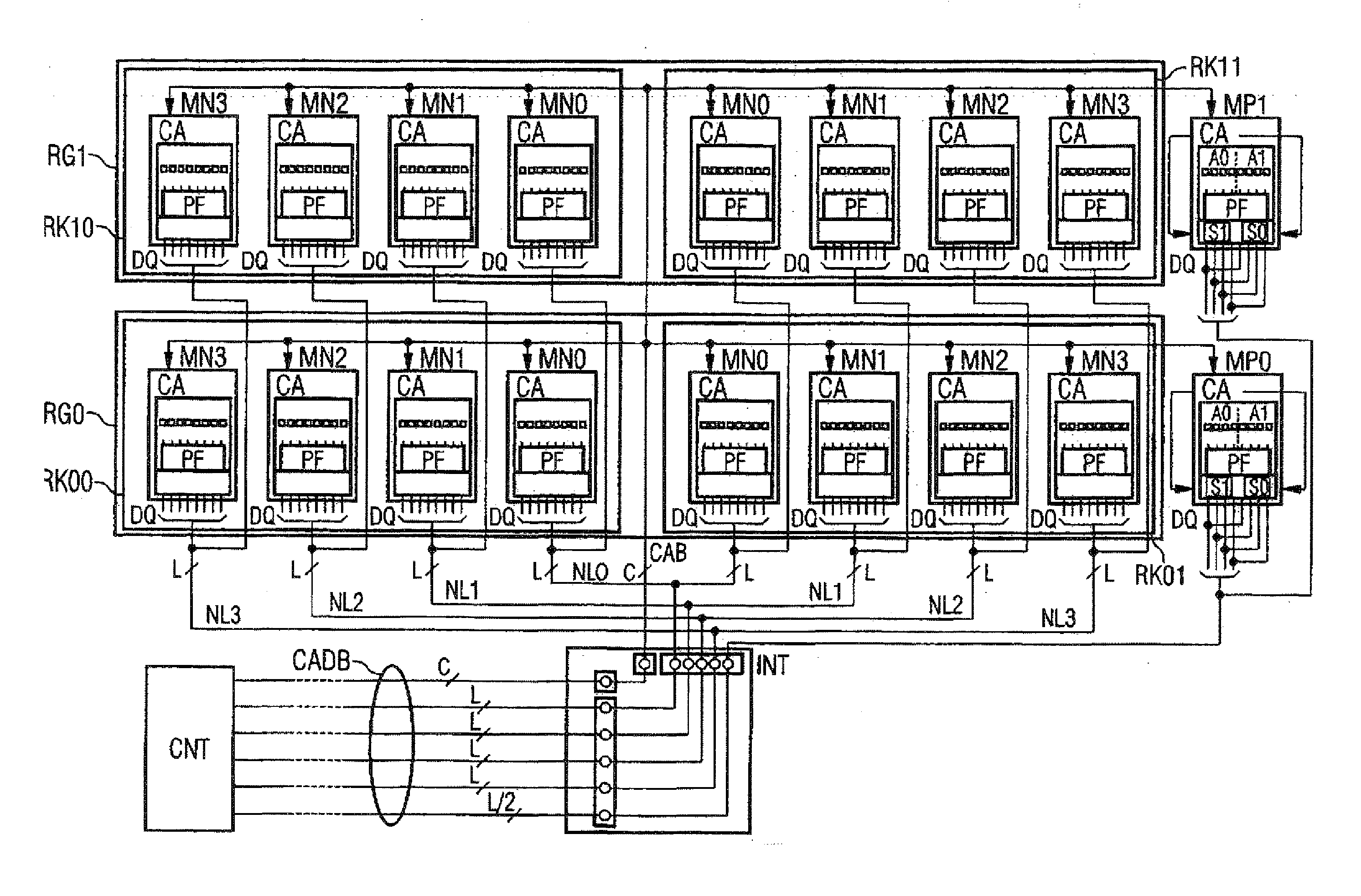
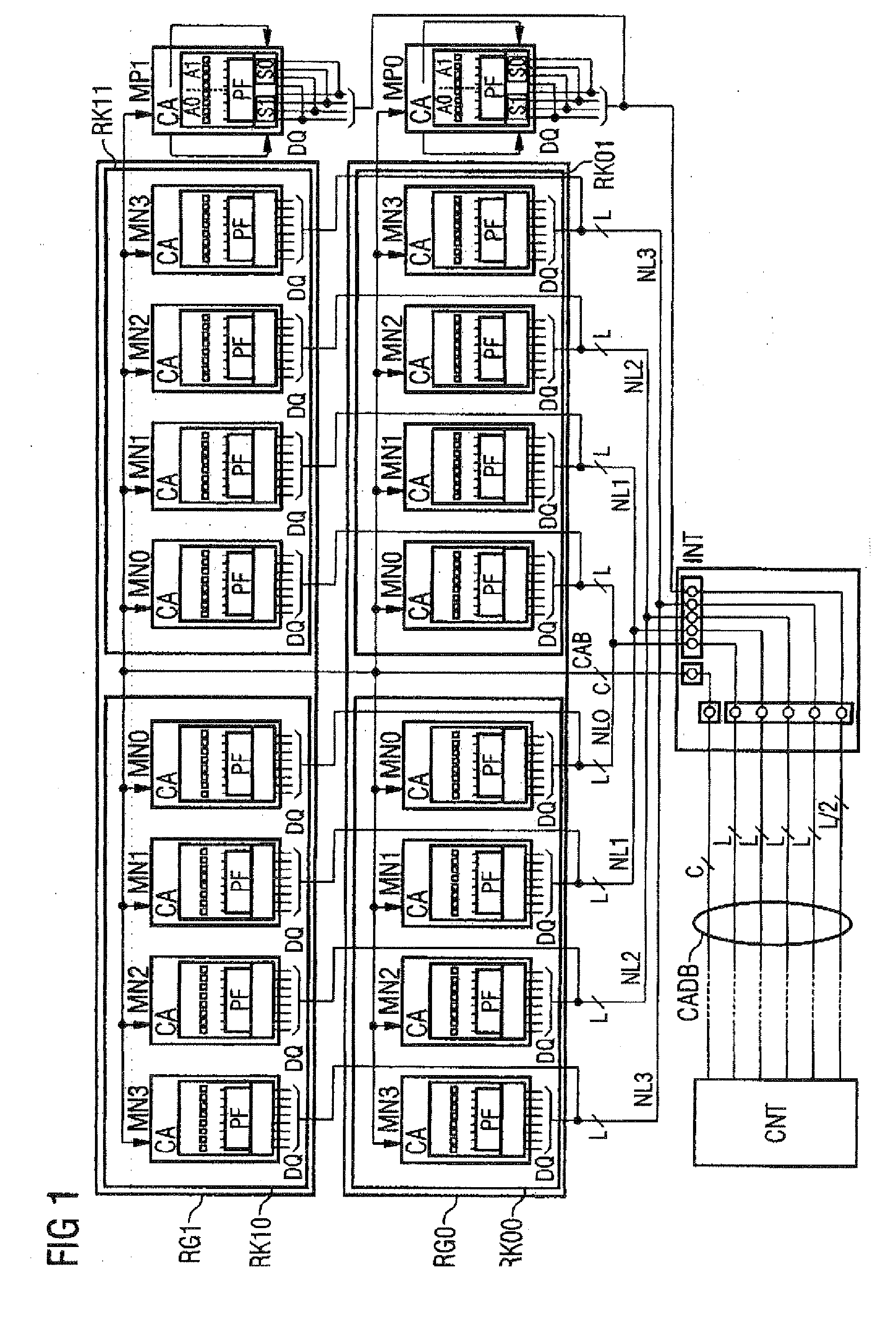
[0035] In FIG. 1, elements of identical type are designated by the same letter combinations each succeeded by a number or number combination for identifying the relevant element. A colon between two numbers denotes the word “to”; thus, e.g. “MN0:3” is to be read as “MN1 to MN4”.

[0036] The memory module illustrated schematically in FIG. 1 contains two rank groups RG0 and RG1, each of which comprises R=2 ranks RK00, RK01 and RK10, RK11, respectively. Each rank contains KN=4 useful bit memory devices MN0:3, each of which has a bidirectional data port DQ with L=8 pins for inputting and outputting a group of L=8 parallel bits which are intended to be written and read at a respectively selected group of L=8 memory cells (L-cell group). The relevant 8-cell group is selected depending on the pattern of a plurality of address bits which are received at assigned pins of a control and address terminal CA. In FIG. 1, in each useful bit memory device, an 8-cell group of this type is symbolicall...


PUM


Abstract

A memory module stores data in the form of code words, each code word comprising useful bits and check bits for error correction. The memory module contains a first group of the memory devices including check bits and a second group of the memory devices including useful bits, the second group memory devices forming ranks, each rank being addressed as a whole, the ranks forming rank groups, each rank group including at least two ranks and a first group memory device. The memory module further contains a connecting device transferring bit packets each containing useful bits and check bits in the parallel format between an interface of the memory module and the memory devices of a selected rank group

Description

CROSS-REFERENCE TO RELATED APPLICATIONS [0001] This application claims foreign priority benefits under 35 U.S.C. §119 to co-pending German patent application number DE 10 2005 053 625.5, filed 10 Nov. 2005. This related patent application is herein incorporated by reference in its entirety. BACKGROUND OF THE INVENTION [0002] 1. Field of the Invention [0003] The invention relates to a memory module containing a plurality of memory devices of the RAM type. As is known, the acronym RAM refers to read / write memories with direct and random access to the memory cells (random access memory). A preferred, but not exclusive, field of application of the invention constitutes memory arrangements comprising dynamic RAM devices (so-called DRAM devices), such as are customary as main memories in computers. [0004] 2. Description of the Related Art [0005] Memory devices usually have a data port with a plurality L of parallel data terminals (data pins) in order to input and output in each case a gro...

Claims


Application Information

Patent Timeline
IPC IPC(8): G11C29/00
CPCG06F11/1012G11C5/04
Inventor RUCKERBAUER, HERMANN
Owner POLARIS INNOVATIONS
Learn More