
Method for manufacturing organic semiconductor composition and transistor, method for manufacturing active matrix device, method for manufacturing electro optical device, and method for manufacturing electronic apparatus

a manufacturing method and semiconductor technology, applied in the direction of electrical devices, solid-state devices, construction, etc., can solve the problem of hard to obtain stable ink, and achieve the effects of high preservation stability, high reliability, and superior characteristics

Active Publication Date: 2007-06-28
E INK CORPORATION
View PDF3 Cites 21 Cited by
  • Summary
  • Abstract
  • Description
  • Claims
  • Application Information

AI Technical Summary

Benefits of technology

[0010] The advantage of the invention is to provide an organic semiconductor composition that can form an organic semiconductor layer having high preservation stability and superior characteristics, a method for manufacturing a transistor providing the transistor with high reliability using the organic semiconductor composition, a method for manufacturing an active matrix device, a method for manufacturing an electro optical device and a method for manufacturing an electronic apparatus.
[0011] Now, aspects of the present invention are described below.
[0012] The organic semiconductor composition according to a first aspect of the invention includes an organic semiconductor material having a structural unit including at least one thiophene ring as a repeating unit, and an organic solvent including cis-decalin.
[0013] The organic semiconductor composition to form an organic semiconductor layer with high preservation stability and superior characteristics is thus obtained.
[0014] In the organic semiconductor composition, the organic solvent preferably includes 15 wt % or more of cis-decalin.

Problems solved by technology

Due to this aggregation, the organic semiconductor material is precipitated, making it hard to obtain stable ink.

Method used


Image

  • Method for manufacturing organic semiconductor composition and transistor, method for manufacturing active matrix device, method for manufacturing electro optical device, and method for manufacturing electronic apparatus
  • Method for manufacturing organic semiconductor composition and transistor, method for manufacturing active matrix device, method for manufacturing electro optical device, and method for manufacturing electronic apparatus
  • Method for manufacturing organic semiconductor composition and transistor, method for manufacturing active matrix device, method for manufacturing electro optical device, and method for manufacturing electronic apparatus

Examples


first embodiment

[0055] A first embodiment of a thin-film transistor manufactured by using an organic semiconductor composition of the invention is now explained.

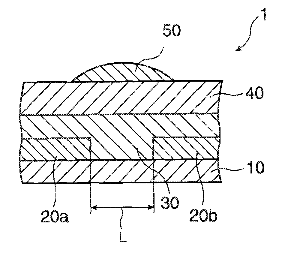
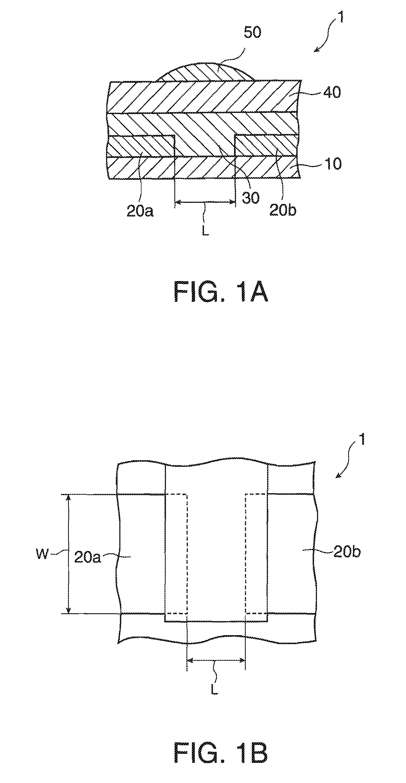
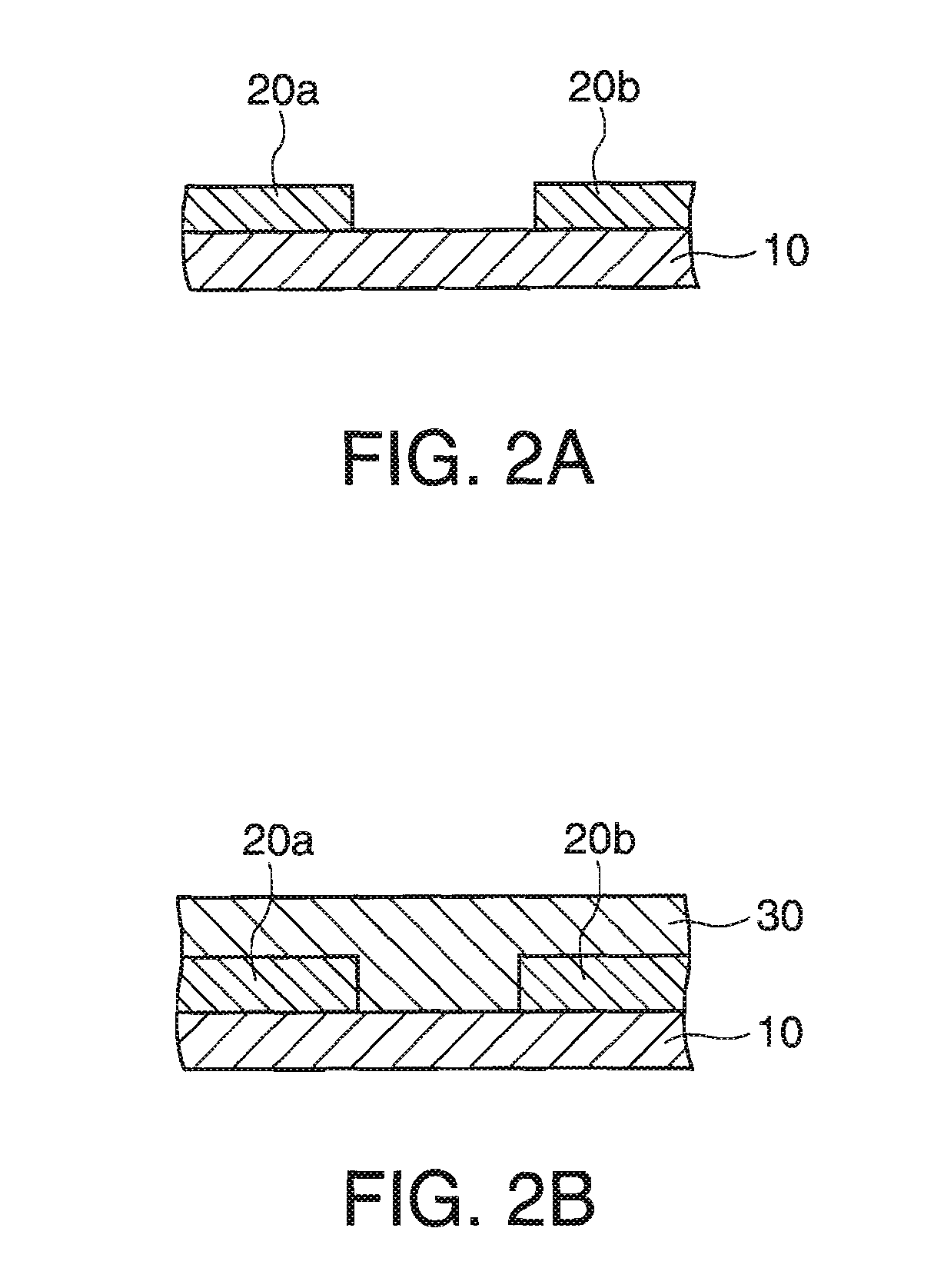
[0056]FIGS. 1A and 1B are schematic views showing the first embodiment of a thin-film transistor manufactured by using the organic semiconductor composition. FIG. 1A is a cross sectional view and FIG. 1B is a plain view. FIGS. 2A, 2B, 3C, and 3D are cross sectional views for explaining a method for manufacturing the thin-film transistor shown in FIGS. 1A and 1B. FIGS. 4A and 4B are schematic views showing three-dimensional structures of cis-decalin and trans-decalin.

[0057] A thin-film transistor 1 (the transistor of the invention) in FIGS. 1A and 1B is a top gate type thin-film transistor formed on a substrate 10, including a source electrode 20a, a drain electrode 20b, an organic semiconductor layer 30, a gate electrode 50 and a gate insulation layer 40. The source electrode 20a is separated from the drain electrode 20b. The organic semi...

second embodiment

[0155] Next, a second embodiment of the thin-film transistor manufactured by using the organic semiconductor composition is explained.

[0156]FIG. 5 is a sectional view schematically showing the second embodiment of the thin-film transistor manufactured by using the organic semiconductor composition.

[0157] The difference of the second embodiment from the first embodiment will be mainly explained, and the same contents of them are omitted.

[0158] A position where each electrode is aligned in the second embodiment is different from the first one. However, other than that is the same as that in the first embodiment.

[0159] As shown in FIG. 5, the thin-film transistor 1 is a bottom gate type thin-film transistor in which the gate electrode 50 is located on the substrate 10 side via the gate insulation layer 40 far from the source electrode 20a and the drain electrode 20b.

[0160] The organic semiconductor layer 30 is formed by using the same organic semiconductor composition as that in t...

examples

[0203] Specific examples of the invention will now be described.

[0204] Preparing liquid materials (organic semiconductor compositions of the invention)

[0205] Liquid materials No. 1 to 48 were prepared as described below.


PUM

PropertyMeasurementUnit
wt %aaaaaaaaaa
lengthaaaaaaaaaa
lengthaaaaaaaaaa

Abstract

An organic semiconductor composition comprises: an organic semiconductor material having a structural unit including at least one thiophene ring as a repeating unit; and an organic solvent including cis-decalin.

Description

BACKGROUND [0001] 1. Technical Field [0002] The present invention relates to a method for manufacturing an organic semiconductor composition and a transistor, a method for manufacturing an active matrix device, a method for manufacturing an electro optical device and a method for manufacturing an electronic apparatus. [0003] 2. Related Art [0004] JP-A-2004-6782 discloses a thin-film transistor formed with an organic semiconductor material, which has recently attracted attention as a device being replaced with a thin-film transistor formed with an inorganic semiconductor material. [0005] As an organic semiconductor material for this thin-film transistor, a polymer organic semiconductor material having thiophene ring is known. The organic semiconductor material provides high carrier mobility and allows an organic semiconductor layer to be formed by a liquid phase process since the polymer can dissolve into an organic solvent to be used as ink. [0006] In the liquid phase process, ink i...

Claims


Application Information

Patent Timeline
Patent Type & Authority Applications(United States)
IPC IPC(8): E04B1/74
CPCH01L51/0007H01L51/0036H01L51/0039H01L51/0043H01L51/0545H10K71/15H10K85/115H10K85/151H10K85/113H10K10/466
Inventor MASUDA, TAKASHI
Owner E INK CORPORATION
Learn More