Nitride semiconductor light emitting device and method of fabricating nitride semiconductor laser device
a technology of nitride semiconductor and laser device, which is applied in the direction of semiconductor lasers, lasers, solid-state devices, etc., can solve the problems of poor light extraction efficiency, and insufficient reliability of conventional nitride semiconductor laser devices
- Summary
- Abstract
- Description
- Claims
- Application Information
AI Technical Summary
Benefits of technology
Problems solved by technology
Method used
Image

Examples
first embodiment
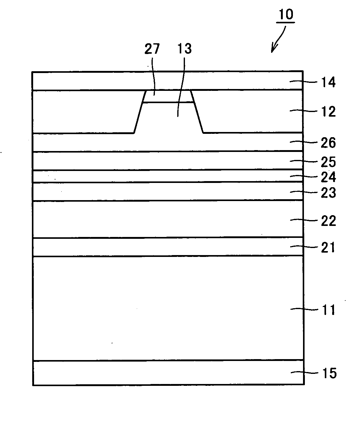
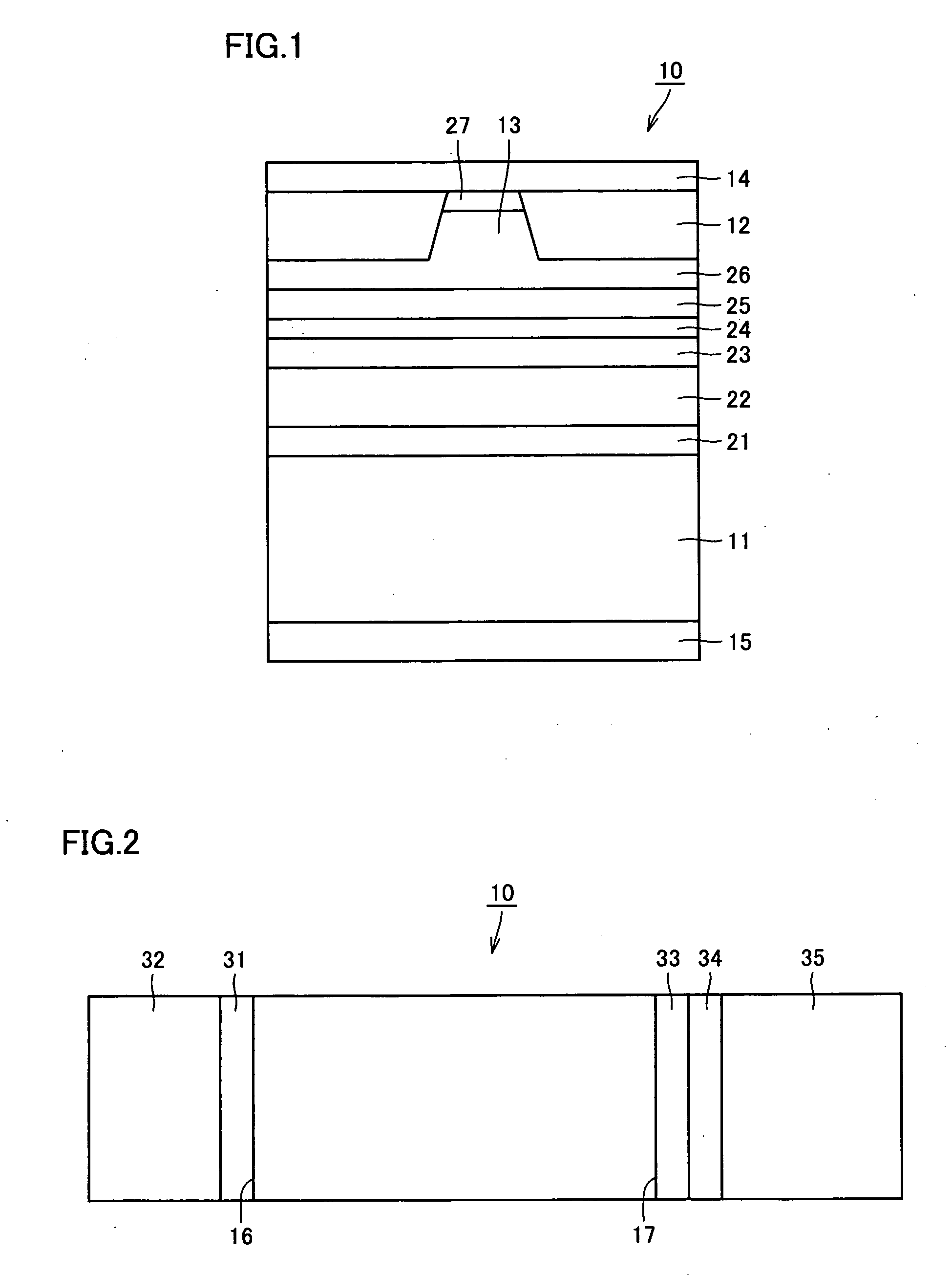
[0039]FIG. 1 is a schematic cross section of one preferred example of a nitride semiconductor laser device of the present embodiment. Herein the present embodiment provides a nitride semiconductor laser device 10 including an n type GaN substrate 11, an n type AlGaInN buffer layer 21 deposited thereon, an n type AlGaInN clad layer 22 deposited thereon, an n type AlGaInN guide layer 23 deposited thereon, an AlGaInN multi quantum well active layer 24 deposited thereon, a p type AlGaInN guide layer 25 deposited thereon, a p type AlGaInN clad layer 26 deposited thereon, and a p type AlGaInN contact layer 27 deposited thereon. It should be noted that each layer has a composition ratio adjusted as appropriate and thus irrelevant to the essence of the present invention. Furthermore in the present embodiment the nitride semiconductor laser device lases at a wavelength which can be adjusted, as appropriate, within a range for example of 370 nm to 470 nm depending on the composition ratio of ...
second embodiment
[0061] The present embodiment provides a nitride semiconductor laser-device similar in configuration to that of the first embodiment except that the cavity has the light emitting facet coated with a coating film modified in configuration.
[0062] Herein in the present embodiment the nitride semiconductor laser device has a cavity with a light emitting facet provided with a 20 nm thick aluminum oxynitride film and thereon a 69 nm thick aluminum oxide film deposited to provide a reflectance of 5%. Note that the aluminum oxynitride film and the aluminum oxide film are deposited in a method and under a condition similar to those described in the first embodiment, and the aluminum oxynitride film contains aluminum, oxygen and nitrogen in amounts of 35 atomic %, 3 atomic % and 62 atomic %, respectively.
[0063]FIG. 7 represents a result of a depthwise AES analysis of a coating film formed of an aluminum oxynitride film deposited on a light emitting facet of a cavity of the nitride semicondu...
third embodiment
[0066] The present embodiment provides a nitride semiconductor laser device similar in configuration to that of the first embodiment except that the cavity has the light emitting facet coated with a coating film modified in configuration.
[0067] Herein in the present embodiment the nitride semiconductor laser device is fabricated as follows: except that the film deposition furnace receives gaseous nitrogen at a flow rate of 1.5 sccm, conditions similar to those described in the first embodiment are adopted, and a 6 nm thick aluminum oxynitride film is deposited as described in the first embodiment, although its content of oxygen is varied, and subsequently thereon a 76 nm thick aluminum oxide film is deposited, similarly as described in the first embodiment.
[0068]FIG. 8 represents a result of a depthwise AES analysis of an aluminum oxynitride film separately provided under the same conditions as described above. As shown in FIG. 8, the aluminum oxynitride film contains aluminum, ox...
PUM
 Abstract
Description
Claims
Application Information
 - R&D
- Intellectual Property
- Life Sciences
- Materials
- Tech Scout
- Unparalleled Data Quality
- Higher Quality Content
- 60% Fewer Hallucinations
Browse by: Latest US Patents, China's latest patents, Technical Efficacy Thesaurus, Application Domain, Technology Topic, Popular Technical Reports.
© 2025 PatSnap. All rights reserved.Legal|Privacy policy|Modern Slavery Act Transparency Statement|Sitemap|About US| Contact US: help@patsnap.com