
Polishing pad and polishing apparatus

Inactive Publication Date: 2007-06-14
EBARA CORP
View PDF31 Cites 21 Cited by
  • Summary
  • Abstract
  • Description
  • Claims
  • Application Information

AI Technical Summary

Benefits of technology

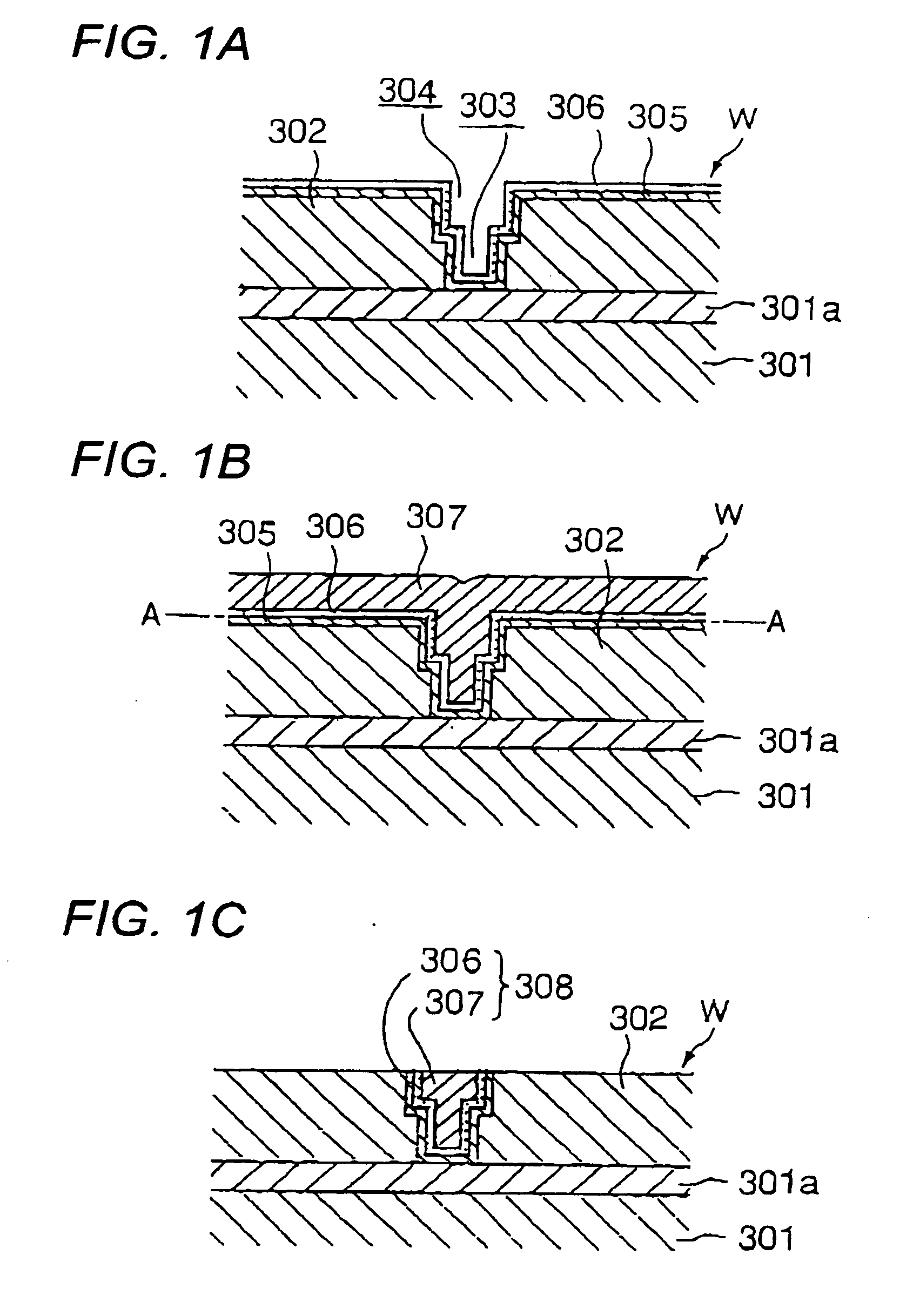
[0011] Dishing or erosion, which can occur in a substrate surface in a polishing process for the formation of fine interconnects, decreases the cross-sectional area of the interconnects and raises the resistance of the interconnects. Dishing or erosion is therefore required to be minimized, especially when forming very fine interconnects of the 65-nm or later generation.
[0064] According to the dresser of the present invention, dressing of a polishing surface of a polishing pad with the dresser can be performed by rubbing the polishing surface with the surface of the diamond dressing section while allowing the tips of the brush bristles provided in the brush dressing section to easily enter, e g., numerous through-holes formed in the polishing pad and scraping out a processing product remaining in the through-holes with the brush bristles. This enables easy and secure removal of foreign matter, such as a polishing product, remaining on the surface (polishing surface) or in the through-holes of the polishing pad.

Problems solved by technology

Such through-holes generally have a low efficiency of passage therethrough of a polishing liquid (electrolytic liquid), and therefore a polishing product and an “old polishing liquid” are likely to remain in the through-holes.
When the polishing product remains in the through-holes and is accumulated on the surface of the processing electrode, the electrical conduction between a substrate and the processing electrode will be impeded by the polishing product, which would cause lowering of polishing characteristics of the polishing apparatus and the stabilities of the characteristics.
It is thus a problem in maintaining the polishing characteristics of the polishing apparatus how to efficiently remove the polishing product and the “old polishing liquid” remaining on the surface of the polishing pad.
Such a polishing pad, however, may contact recessed portions in a surface of a film of interconnect metal or interconnect recesses whereby the recessed portions will be polished, which would cause dishing or erosion.
A large surface roughness of a polishing pad thus lowers the flattening property of the polishing pad.
A polishing pad having a small surface roughness, on the other hand, is poor in the capability of holding a polishing agent (slurry) used in a polishing process.
Thus, a small surface roughness of polishing pad decreases the polishing rate and adversely affects the uniformity of the polishing rate in a surface of a substrate.
It is therefore a significant problem how to condition a surface of a polishing pad in order to polish a substrate without dishing or erosion while maintaining the intended polishing rate and its uniformity in the surface of the substrate.
When processing a fragile material, such as a low-K material, in a semiconductor device manufacturing process, there is a fear of breakage of the material, for example, due to buckling.
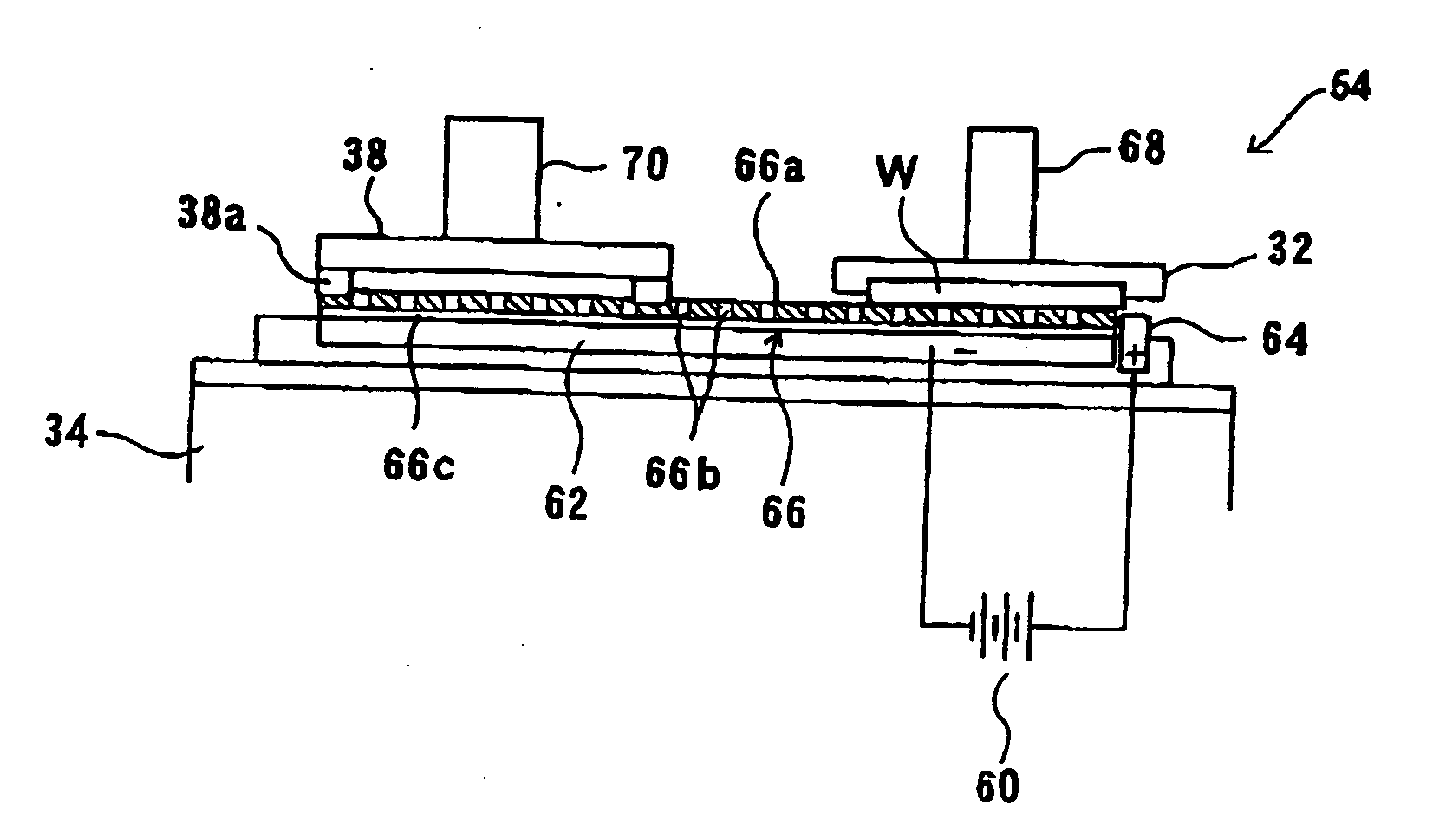
In electrochemical mechanical polishing which generally performs polishing of a conductive film of a substrate by rubbing a polishing pad against the conductive film while applying a voltage between the conductive film and a counter electrode, there is a possibility of breakage of a material due to a load applied by contact between the conductive film of the substrate and the polishing pad and also to a load applied by contact between the substrate and a feeding electrode for feeding electricity to the conductive film of the substrate.

Method used


Image

  • Polishing pad and polishing apparatus
  • Polishing pad and polishing apparatus
  • Polishing pad and polishing apparatus

Examples


experimental example

[0192] A 100 mm-diameter dresser A with diamond abrasive grains electrodeposited on a surface and a 100 mm-diameter dresser B with diamond abrasive grains, having a higher grain count (smaller size) than the abrasive grains of the dresser A, electrodeposited on a surface, were prepared. A polishing pad composed of IC-1000, manufactured by Nitta Haas Inc., was dressed (conditioned) with the dresser A at a pressure of 3.2 psi. The same polishing pad was dressed with the dresser B at a pressure of 0.64 psi. Dressing of the same polishing with the dresser B was also carried out but at a different pressure of 0.4 psi. Polishing of a surface of a substrate (semiconductor wafer) was carried out using each of the dressed polishing pads, and a change in a surface level difference with the progress of polishing was measured on each of the test substrates to examine a difference in the fattening characteristic between the substrates. In the experiment a load of 25 N (including the own weight o...


PUM

PropertyMeasurementUnit
Fractionaaaaaaaaaa
Fractionaaaaaaaaaa
Pressureaaaaaaaaaa

Abstract

A polishing pad enables efficient removal of a polishing product and an “old polishing liquid” remaining on a surface (polishing surface) or in through-holes of a polishing pad. The polishing pad has a polishing surface and a plurality of through-holes extending in the thickness direction, which communicate with each other by communication grooves. The through-holes have a diameter of, e.g., 2 to 5 mm. The aperture ratio of the through-holes is, e.g., 10 to 50% of the surface area of the polishing surface of the polishing pad. The depth of the communication grooves is, e.g., 40 to 60% of the thickness of the polishing pad. The width of the communication grooves is, e.g., 10 to 50% of the diameter of the through-holes.

Description

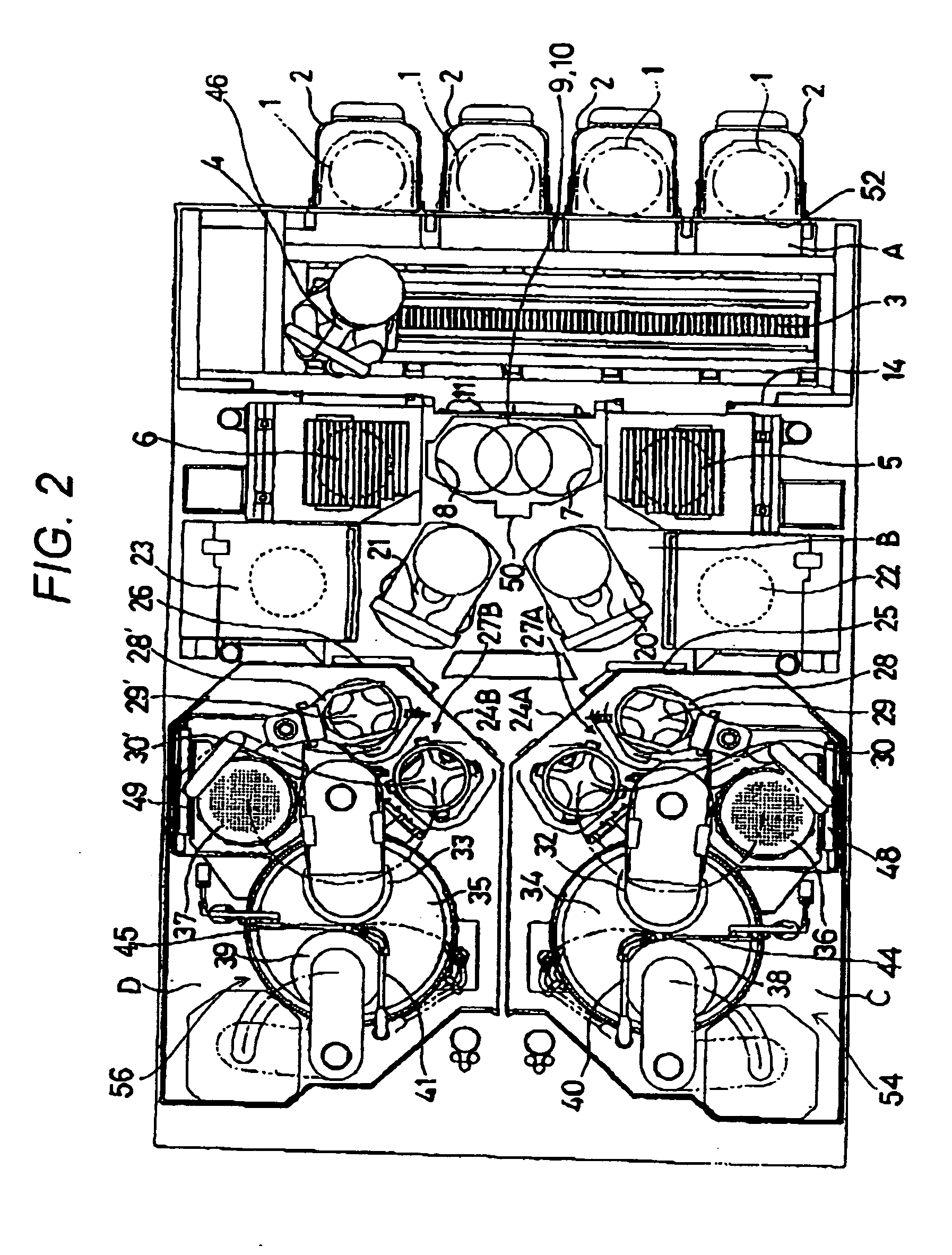
BACKGROUND OF THE INVENTION [0001] 1. Field of the Invention [0002] The present invention relates to a polishing pad and a polishing apparatus, and more particularly to a polishing pad useful for polishing an interconnect material (metal), such as copper, deposited on a substrate, such as a semiconductor wafer, and embedded in fine interconnect recesses provided in an insulating film (interlevel dielectric film) formed on the substrate, thereby forming interconnects, and to a polishing apparatus that uses the polishing pad. [0003] The present invention also relates to a method for conditioning a polishing pad of a polishing apparatus, and to a polishing apparatus and a polishing method which are useful for processing a film of conductive material formed on a substrate, such as a semiconductor wafer, or removing impurities adhering to the surface of the substrate. [0004] The present invention also relates to a dresser for dressing a polishing pad of a polishing apparatus, a polishing...

Claims


Application Information

Patent Timeline
IPC IPC(8): B24B1/00B24B29/00B24D11/00
CPCB24B37/26B24B53/017
Inventor KOBATA, ITSUKIKOHAMA, TATSUYA
Owner EBARA CORP
Learn More