
Method and apparatus for generating OPC rules for placement of scattering bar features utilizing interface mapping technology

a technology of interface mapping and feature placement, applied in special data processing applications, optics, instruments, etc., can solve the problems of reducing the size of an integrated circuit, cd (critical dimension) of its corresponding mask pattern approaching the resolution limit of the optical exposure tool, and still be a difficult process, so as to improve the performance of sb placement

Inactive Publication Date: 2007-05-31
ASML NETHERLANDS BV
View PDF7 Cites 6 Cited by
  • Summary
  • Abstract
  • Description
  • Claims
  • Application Information

AI Technical Summary

Benefits of technology

[0011] In an effort to solve the foregoing needs, it an object of the present invention to provide a rule-based approach for applying scattering bars to a mask design, which utilizes the interference map in the rule formation process, so as to take advantage of and incorporate the improved performance regarding SB placement associated with the interference mapping technique.
[0018] The method of the present invention provides important advantages over the prior art. Most importantly, the rule-based approach of the present invention for applying scattering bars to a mask design, which utilizes the interference map in the rule formation process, simplifies the process of applying the scattering bars to the mask design, and allows for a robust application of scattering bars to the design without requiring a significant amount of calculations to be performed by the CAD system, thereby minimizing the amount of time required to complete the design process. Further, the method also allows for rapid determination of the locations to apply scattering bars in areas not necessarily identified by the interference map to require scattering bars.

Problems solved by technology

These rules are set by processing and design limitations.
As the size of an integrated circuit is reduced and its density increases, however, the CD (critical dimension) of its corresponding mask pattern approaches the resolution limit of the optical exposure tool.
While the concept has been demonstrated feasible for manufacturing purposes, it can still be a challenging process to apply the concepts into a manufacturing worthy implementation, especially when dealing with complex mask designs.
For example, current techniques for applying scattering bars to a mask design can be a time consuming process due to the complexities of today's current masks.
This problem can be exacerbated when the scattering bars are placed in the mask design utilizing interference mapping techniques identified above.

Method used


Image

  • Method and apparatus for generating OPC rules for placement of scattering bar features utilizing interface mapping technology
  • Method and apparatus for generating OPC rules for placement of scattering bar features utilizing interface mapping technology
  • Method and apparatus for generating OPC rules for placement of scattering bar features utilizing interface mapping technology

Examples


Embodiment Construction

[0033] As explained in more detail below, the rule-based approach of the present invention for applying scattering bars to a mask design, which utilizes the interference map in the rule formation process, simplifies the process of applying the scattering bars to the mask design, and allows for a robust application of scattering bars to the design without requiring a significant amount of calculations to be performed by the CAD system, thereby minimizing the amount of time required to complete the design process. Further, the method also allows for rapid determination of the locations to apply scattering bars in areas not necessarily identified by the interference map to require scattering bars.

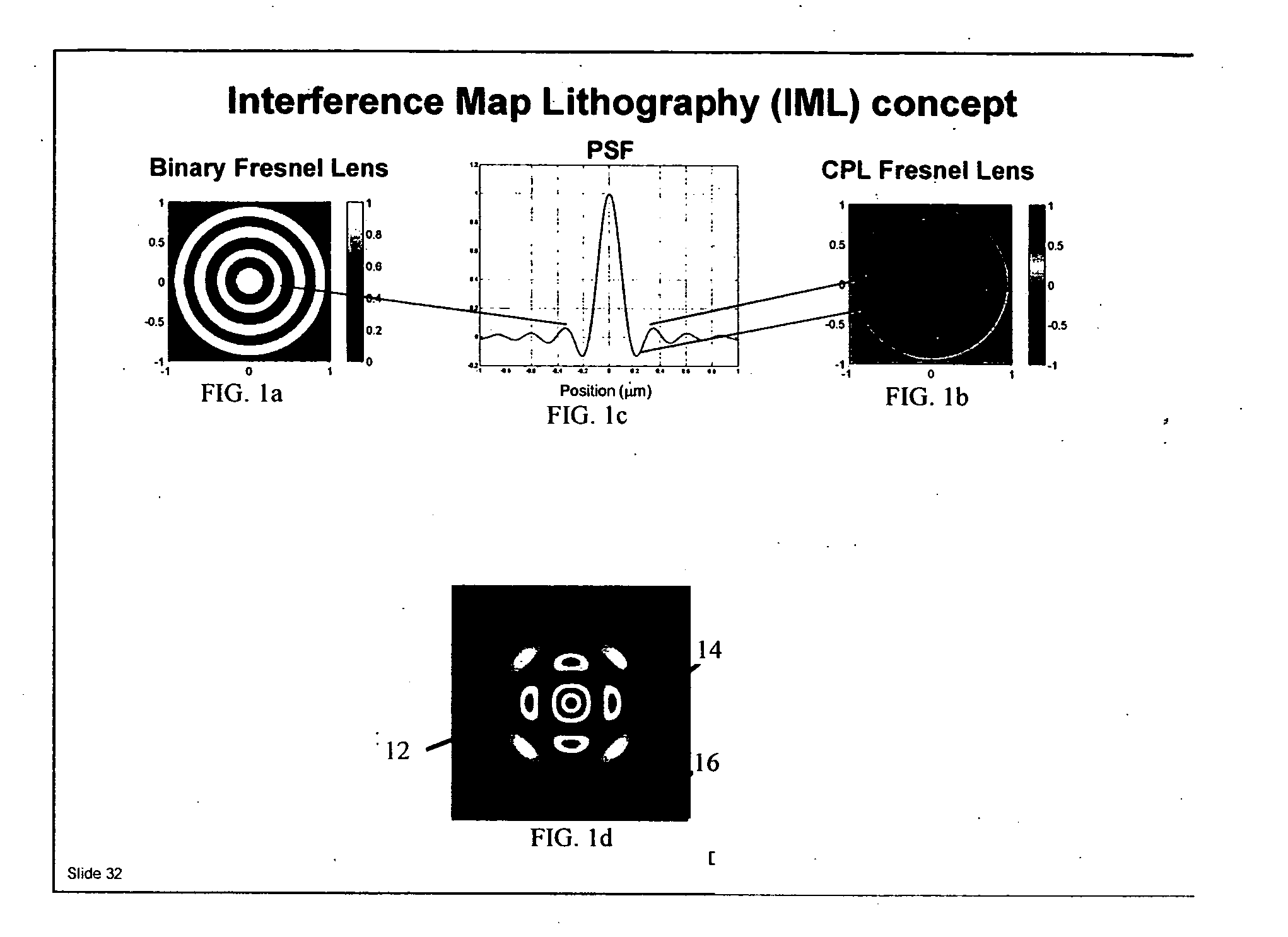
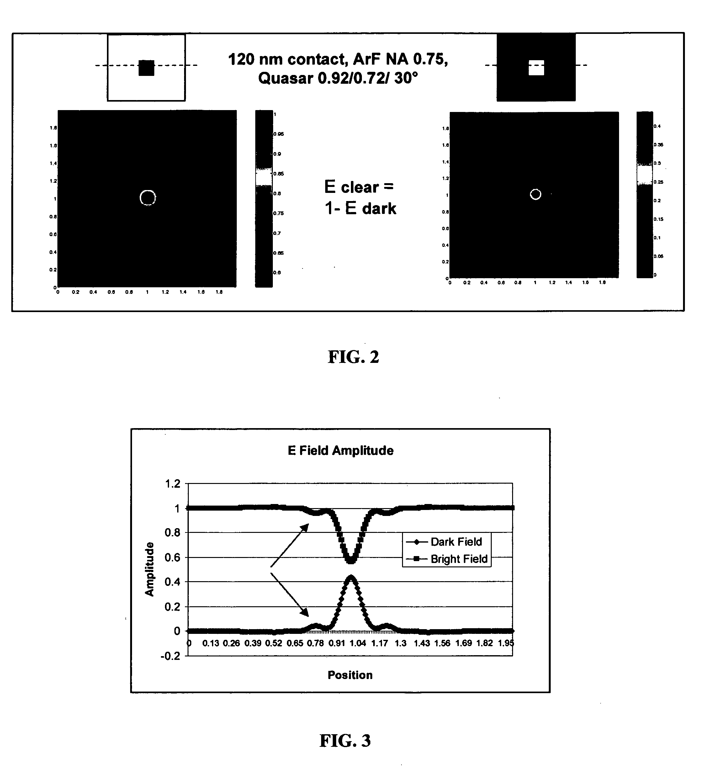
[0034]FIGS. 1a-1d illustrates an example of the generation of an interference map for an isolated contact illuminated using Quasar™ illumination, which can be generated using either an empirical method or a simulation method as detailed in U.S. patent application Ser. Nos. 10 / 756,829 filed on...


PUM

PropertyMeasurementUnit
wavelengthaaaaaaaaaa

Abstract

A method of applying optical proximity correction features to a mask having a plurality of features to be imaged. The method includes the steps of defining a set of process parameters to be utilized to image the mask; defining a set of pitch ranges corresponding to pitches exhibited by the plurality of features to be imaged; determining an interference map for at least one of the pitch ranges; and generating a set of rules for positioning scattering bars adjacent the plurality of features based on the interference map, where the set of rules governs scattering bar placement for features having a pitch which falls within the pitch range utilized to generate the interference map.

Description

CLAIM OF PRIORITY [0001] This patent application, and any patent(s) issuing therefrom, claims priority from U.S. provisional patent application No. 60 / 734,317, filed on Nov. 8, 2005, entitled “Method Of Generating OPC Rules With Interference Mapping”, which is incorporated herein by reference in its entirety.FIELD OF THE INVENTION [0002] The present invention relates to photolithography, and in particular relates to a method of generating a rule-base for applying optical proximity correction features to mask layouts utilizing an interference map. In addition, the present invention relates to a device manufacturing method using a lithographic apparatus comprising a radiation system for providing a projection beam of radiation; a mask table for holding a mask, serving to pattern the projection beam; a substrate table for holding a substrate; and a projection system for projecting the patterned projection beam onto a target portion of the substrate. BACKGROUND OF THE INVENTION [0003] L...

Claims


Application Information

Patent Timeline
Patent Type & Authority Applications(United States)
IPC IPC(8): G06F17/50G03F1/00
CPCG03F1/144G03F1/36
Inventor VAN DEN BROEKE, DOUGLASPARK, SANGBONGHSU, CHUNG-WEICHEN, JANG FUNG
Owner ASML NETHERLANDS BV
Learn More