
Semiconductor die package using leadframe and clip and method of manufacturing

Inactive Publication Date: 2007-05-24
SEMICON COMPONENTS IND LLC
View PDF35 Cites 108 Cited by
  • Summary
  • Abstract
  • Description
  • Claims
  • Application Information

AI Technical Summary

Benefits of technology

[0066] Embodiments of the invention provide for a number of advantages. For example, embodiments of the invention can have the same footprint and pin assignment as other types of conventional packages, while also exhibiting good electrical and thermal performance. In addition, the methods according to embodiments of the invention may use alignment structures to align clip structures on top of a semiconductor die with a leadframe structure at the bottom of the semiconductor die. This results in more efficient processing, and flip chip attachment processes need not be performed in embodiments of the invention. Also, embodiments of the invention are robust. In some embodiments, the semiconductor dies are not exposed to the environment.

Problems solved by technology

Also, when producing wireless packages, it is often difficult to create a clip (e.g., a source clip) that has a deep downset.
Another problem that exists is the problem of applying inconsistent or uneven amounts of solder between the clip and the semiconductor die.
When inconsistent or uneven amounts of solder are used between a die and a clip, the resulting packages may exhibit poor performance.

Method used


Image

  • Semiconductor die package using leadframe and clip and method of manufacturing
  • Semiconductor die package using leadframe and clip and method of manufacturing
  • Semiconductor die package using leadframe and clip and method of manufacturing

Examples


Embodiment Construction

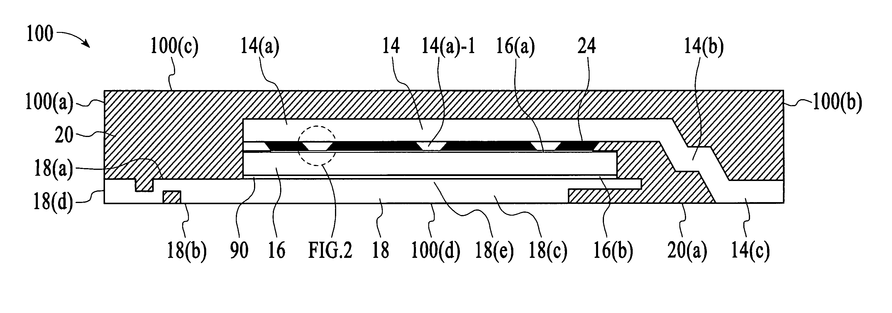
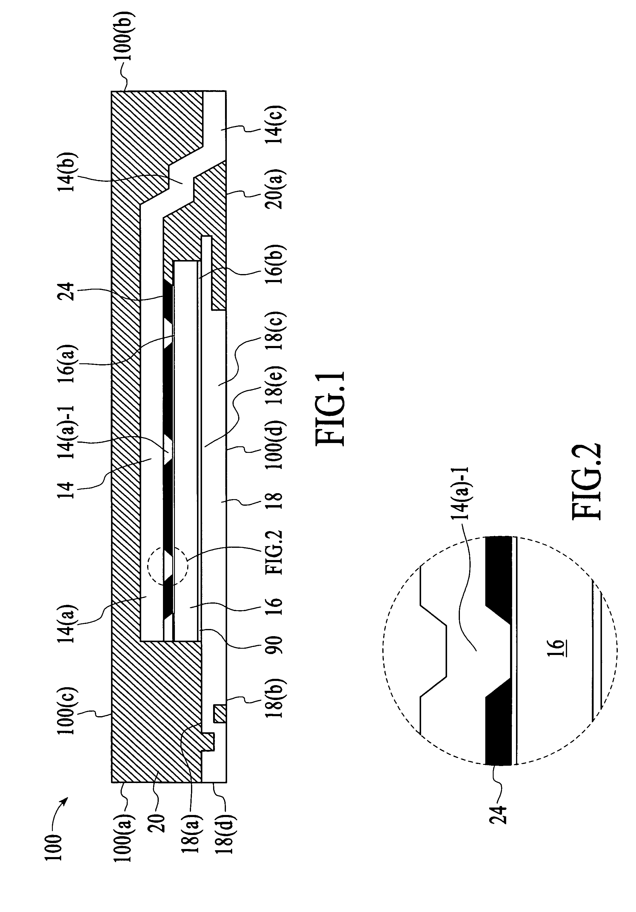
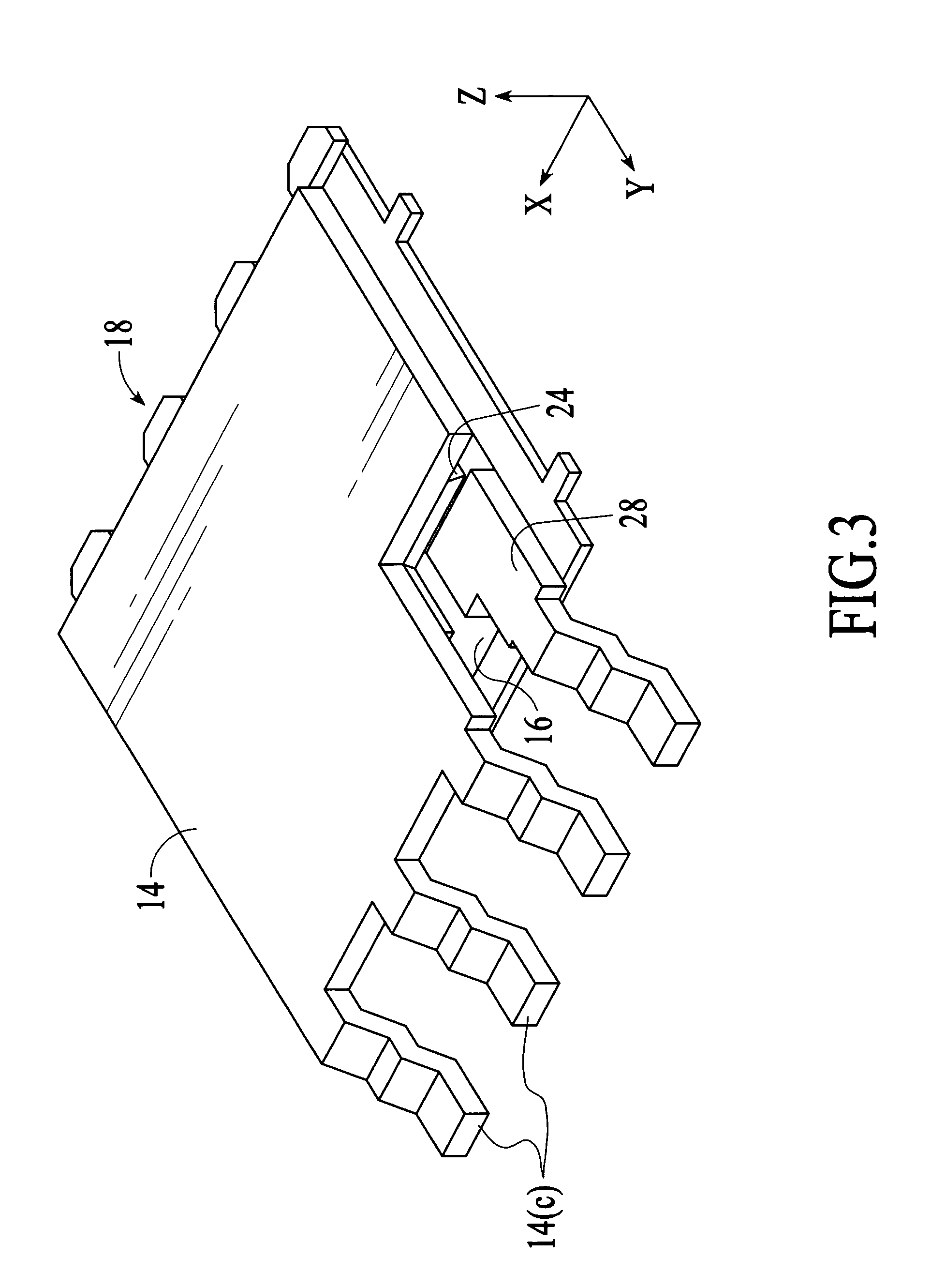
[0028] Embodiments of the invention can include wireless packages. A wireless package according to an embodiment of the invention does not use wires to connect to input and / or output terminals of an electrical device in a semiconductor die. In other embodiments, the semiconductor die packages need not be wireless. For example, as illustrated below, embodiments of the invention include unique source clip structures with specific configurations. Such source clip structures could be used in a semiconductor die package with a gate wire bond. However, wireless semiconductor die packages are preferred as they generally have better thermal and electrical properties than semiconductor die packages that use wires for terminal connections.

[0029] In one semiconductor die package embodiment, the semiconductor die package comprises a clip structure comprising a major portion, at least one pedestal extending from the major portion, a downset portion, and a lead portion. The downset portion is be...


PUM


Abstract

A clip structure for a semiconductor package is disclosed. The clip structure includes a major portion, at least one pedestal extending from the major portion, a downset portion, and a lead portion. The downset portion is between the lead portion and the major portion. The clip structure can be used in a MLP (micro-leadframe package).

Description

CROSS-REFERENCES TO RELATED APPLICATIONS [0001] NONE BACKGROUND OF THE INVENTION [0002] Many semiconductor die packages use clips instead of wires to form external connections to external terminals. Such semiconductor die packages are sometimes referred to as “wireless” packages. A typical wireless package includes a clip that is attached to a semiconductor die. Wireless packages generally have better electrical and thermal performance than packages that use wire-based electrical connections. [0003] Typically, conventional wireless packages need to be designed into a customers' circuit boards, because the circuit boards have unique footprints and pin assignments. It would be desirable to provide for a semiconductor die package that has a footprint and pin assignment that can correspond to conventional package footprints and pin assignments, while still having good electrical and thermal performance. [0004] Also, when producing wireless packages, it is often difficult to create a cli...

Claims


Application Information

Patent Timeline
IPC IPC(8): A47G1/10
CPCH01L21/561H01L21/568H01L21/6835H01L23/49548H01L23/49551H01L23/49562H01L24/33H01L24/36H01L24/39H01L24/83H01L24/97H01L2224/29111H01L2224/32057H01L2224/32245H01L2224/83385H01L2224/83801H01L2224/97H01L2924/01005H01L2924/01013H01L2924/01029H01L2924/01033H01L2924/01047H01L2924/01049H01L2924/0105H01L2924/01057H01L2924/01078H01L2924/01082H01L2924/01327H01L2924/0781H01L2924/13091H01L2924/19043H01L2224/2919H01L2924/01006H01L2924/014H01L2924/0665H01L2924/15747H01L2924/12041H01L2224/29109H01L2224/29116H01L2224/16245H01L2224/73253H01L2924/3651H01L2224/37147H01L2924/1306H01L2924/12032H01L2924/1305H01L2224/83H01L2924/00H01L2924/00014H01L2924/181H01L24/37H01L2224/8485H01L2924/18301H01L2224/0603H01L2924/00012H01L23/50H01L23/48
Inventor VICTOR R. CRUZ, ERWINCABAHUG, ELSIECHING SHIAN, TIIYER, VENKAT
Owner SEMICON COMPONENTS IND LLC
Learn More