
Zeolite sol and method for preparing the same, composition for forming porous film, porous film and method for forming the same, interlevel insulator film, and semiconductor device

a technology of zeolite sol and zeolite, which is applied in the field of zeolite sol and method for preparing the same, which can solve the problems of increasing the interconnection delay time, hindering the enhancement of the performance of the semiconductor circuit, and increasing the cost of the siloxane polymer synthesis precursor solution, and achieves low dielectric constant, high film consistency, and mechanical strength sufficient

Inactive Publication Date: 2007-05-17
SHIN ETSU CHEM IND CO LTD +1
View PDF4 Cites 11 Cited by
  • Summary
  • Abstract
  • Description
  • Claims
  • Application Information

AI Technical Summary

Benefits of technology

The present invention provides a method for preparing a zeolite sol that can be easily thinned to an intended thickness and has excellent mechanical strength, dielectric properties, adhesion, and film consistency. The zeolite sol can be added to a composition for forming a porous film, which can be used in semiconductor fabrication processes. The composition for forming a porous film contains the zeolite sol and a composition containing a silicon-containing compound. The resulting porous film has improved mechanical strength and dielectric properties. The present invention also provides a composition for forming a porous film that can be easily prepared and has improved mechanical strength and dielectric properties.

Problems solved by technology

In the fabrication of semiconductor integrated circuits, as the circuits are packed tighter, an increase in interconnection capacitance, which is a parasitic capacitance between metal interconnections, leads to an increase in interconnection delay time, thereby hindering the enhancement of the performance of semiconductor circuits.
However, use of this structure alone has limits in the enhancement of the performance, so the reduction in interconnection capacitance is an urgent necessity for higher performance of semiconductors.
However, these methods have respective major drawbacks as follows.
In the first method for forming a porous film, the synthesis of the precursor solution of the siloxane polymer increases the cost.
In addition, the formation of the coating film by coating the precursor solution increases the amount of silanol groups remaining in the coating film, which causes degassing phenomenon indicating the evaporation of water and the like in the heat treatment process that is conducted later and which also deteriorates the film quality due to the porous film absorbing humidity.
In the second method for forming a porous film, the speed control of the evaporation of the solvent from the wet gel requires a special type of coating device, which increases the cost.
In addition, a significant amount of silanol remains on the surface of the micro-pores which must be silanized because otherwise hygroscopicity is high and the film quality decreases.
The silanization makes the process more complicated.
In the case where a wet gel is formed by the CVD process, it is necessary to use a special type of CVD device which is different from the plasma CVD device generally used in the semiconductor process, thereby also increasing the cost.
This makes it difficult to set the relative permittivity of the porous film to 2 or below.
However, it is not preferable because it makes the manufacturing process complicated and increases the cost.
However, these methods have problems as follows.
In the former method, a powdered porous member can be easily formed, but it is impossible to form a porous film as a thin film on a substrate which is used for the fabrication of semiconductor devices.
In the latter method, a porous member can be formed into a thin film, but it is impossible to control the orientation of micro-pores, and it is also impossible to form a uniform thin film in a wide area.
However, in this method, too, the restriction of the solute concentration makes it difficult to properly control the thickness of a coating film, thereby making it difficult to apply it to a practical semiconductor fabrication process.
When this solution is diluted with water, the thickness of the coating film becomes controllable, but the speed of polycondensation of the silica component increases to lose stability of the coating solution.
However, these methods form a zeolite film in a sealed container such as an autoclave, and are not practically used in a fabrication process for semiconductor devices.
Because it is considered that a coefficient of elasticity must be 5 GPa or higher for use in the actual semiconductor fabrication process, these inventions cannot be said to be satisfactory for mechanical strength.
As described above, the conventional porous films have problems wherein the film consistency is low and the thickness is not properly controllable, and as a result, it is difficult even to prepare a coating film from the material using zeolite sol.
Therefore, when a porous film using the conventional zeolite sol is integrated into multilayered interconnections of a semiconductor device as an insulator film, the porous film is difficult to be thinned, the film consistency is low, and the film thickness is not properly controllable.
These problems decrease the yield of the semiconductor device fabrication or make the fabrication itself difficult.
Furthermore, a porous film with a low mechanical strength deteriorates the reliability of the semiconductor device, even if it can be used for semiconductor fabrication.

Method used


Image

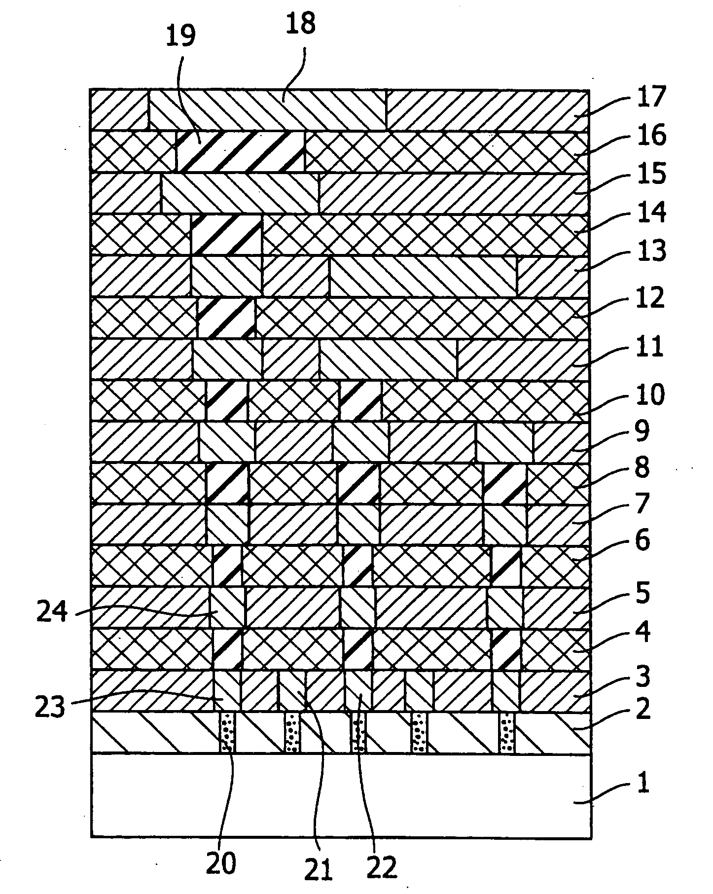
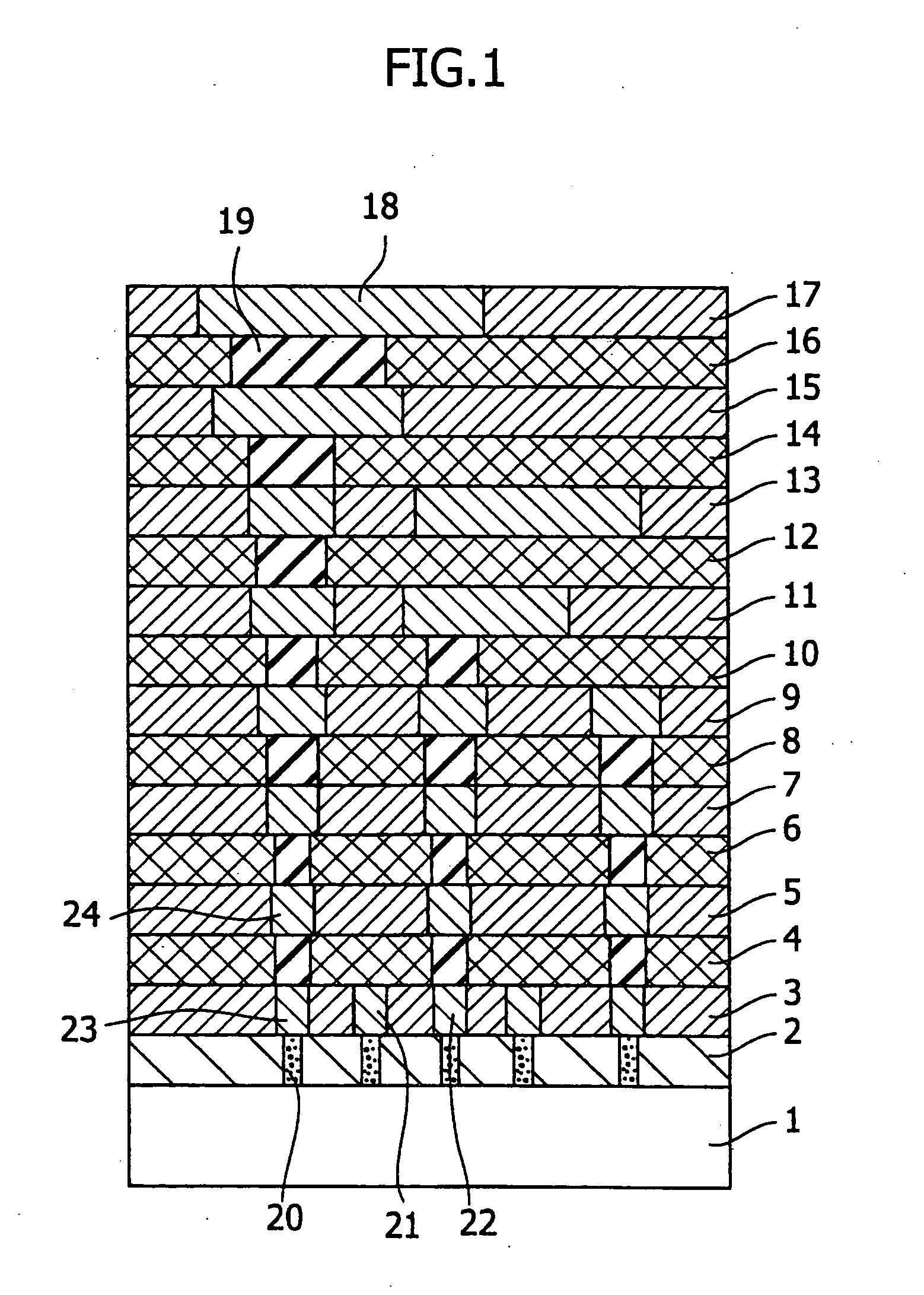
  • Zeolite sol and method for preparing the same, composition for forming porous film, porous film and method for forming the same, interlevel insulator film, and semiconductor device
  • Zeolite sol and method for preparing the same, composition for forming porous film, porous film and method for forming the same, interlevel insulator film, and semiconductor device

Examples


example 2

[0107] Another zeolite sol was prepared in the same manner as in Example 1 except that 210 g of aqueous solution of 1 mol / L tetrabutylammonium hydroxide was used instead of 163 g of aqueous solution of 1 mol / L tetrapropylammonium hydroxide.

example 3

[0108] Another zeolite sol was prepared in the same manner as in Example 1 except that 94 g of tetraethoxysilane was used instead of 69 g of tetramethoxysilane.

example 4

[0109] A mixture of 69 g of tetramethoxysilane and 66 g of methanol was dropped over 1 hour at 40° C. into a mixture of 65 g of 40 wt % aqueous methylamine solution of, 30 g of ultra pure water, 430 g of methanol and 163 g of aqueous solution of 1 mol / L tetrapropylammonium hydroxide. The resultant solution was condensed at 40 to 45° C., and the reaction mixture was stirred for 24 hours at 75° C. so as to obtain a zeolite sol.

[0110] In the following Coating Examples 1 to 4, the zeolite sols obtained in Examples 1 to 4 were added to a base component to prepare a composition for forming a porous film. Then, a porous film was formed and its physical properties were measured by the following methods.

1. Relative Permittivity

[0111] Relative permittivity was measured by a CV method with an automatic mercury probe, by using a 495 CV Measurement System (from SSM Japan).

2. Coefficient of Elasticity

[0112] Coefficient elasticity was measured by using a nano indicator (from Nano Instrument...


PUM

PropertyMeasurementUnit
particle diameteraaaaaaaaaa
temperatureaaaaaaaaaa
relative permittivityaaaaaaaaaa

Abstract

The present invention provides a zeolite sol which can be formed into a porous film that can be thinned to an intended thickness by a method used in the ordinary semiconductor process, that excels in dielectric properties, adhesion, film consistency and mechanical strength, and that can be easily thinned; a composition for film formation; a porous film and a method for forming the same; and a high-performing and highly reliable semiconductor device which contains this porous film inside. More specifically, the zeolite sol is prepared by hydrolyzing and decomposing a silane compound expressed by a general formula: Si(OR1)4 (wherein R1 represents a straight-chain or branched alkyl group having 1 to 4 carbons, and when there is more than one R1, the R1s can be independent and the same as or different from each other) in a conventional coating solution for forming a porous film in the presence of a structure-directing agent and a basic catalyst; and then by heating the silane compound at a temperature of 75° C. or lower. A composition for forming a porous film which contains this zeolite sol is used.

Description

RELATED APPLICATIONS [0001] This application is a divisional application of U.S. application Ser. No. 10 / 703,854 filed on Nov. 7, 2003, which claims priority from Japanese Patent Application No. 2003-329129 filed on Nov. 13, 2002, the disclosures of which are incorporated by reference herein in their entirety.BACKGROUND OF THE INVENTION [0002] I. Field of the Invention [0003] The present invention relates to a zeolite sol which can be formed into a porous film that excels in dielectric properties, adhesion, film consistency and mechanical strength; a composition for film formation; a porous film and a method for forming the same; and a semiconductor device which contains the porous film inside. [0004] 2. Description of the Related Art [0005] In the fabrication of semiconductor integrated circuits, as the circuits are packed tighter, an increase in interconnection capacitance, which is a parasitic capacitance between metal interconnections, leads to an increase in interconnection del...

Claims


Application Information

Patent Timeline
Patent Type & Authority Applications(United States)
IPC IPC(8): C23C16/00C07C5/25H01L23/12C01B39/04H01L21/312H01L21/316H01L21/768H01L23/522
CPCC01B39/04H01L21/02126H01L21/31695H01L21/02216H01L21/02282H01L21/02203
Inventor OGIHARA, TSUTOMUYAGIHASHI, FUJIONAKAGAWA, HIDEOSASAGO, MASARU
Owner SHIN ETSU CHEM IND CO LTD
Learn More