
Method And Apparatus For Detecting The Endpoint Of A Chemical-Mechanical Polishing Operation

a technology of chemical-mechanical polishing and endpoint detection, which is applied in the direction of semiconductor/solid-state device testing/measurement, lapping machines, instruments, etc., can solve the problems of increasing the chance of damaging the surface of the polished layer, reducing the production rate of cmp equipment, and changing the endpoin

Inactive Publication Date: 2007-05-10
ADVANCED MICRO DEVICES INC
View PDF8 Cites 29 Cited by
  • Summary
  • Abstract
  • Description
  • Claims
  • Application Information

AI Technical Summary

Benefits of technology

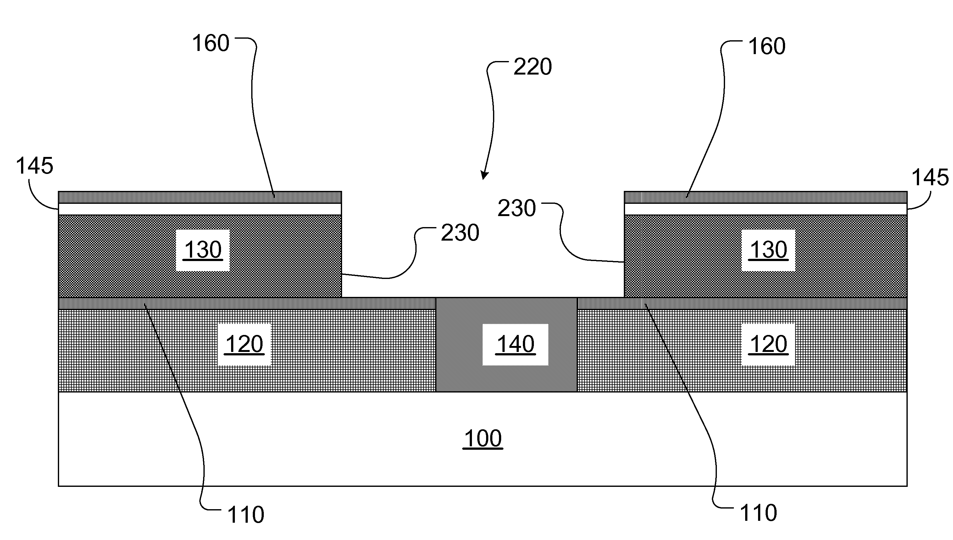
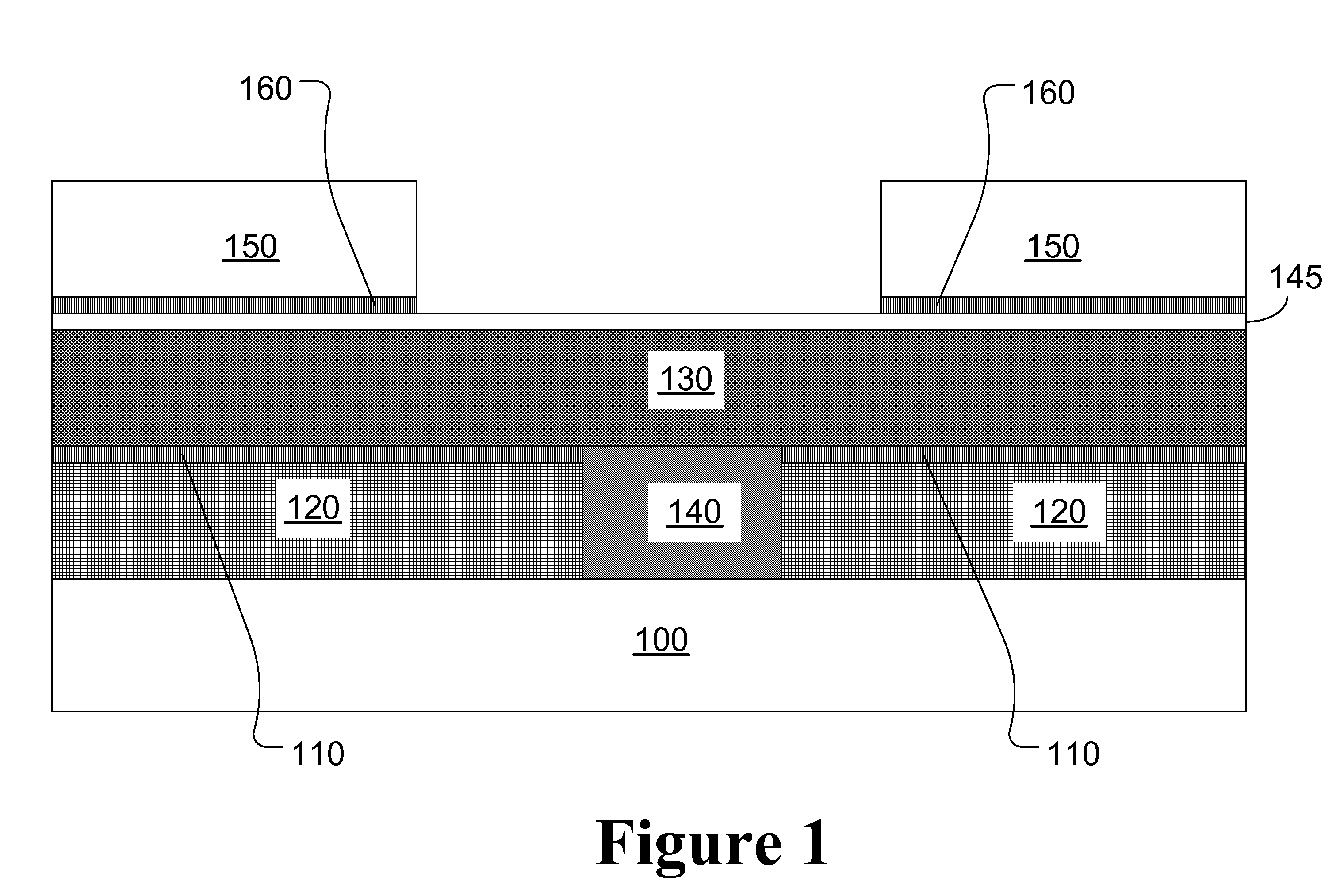
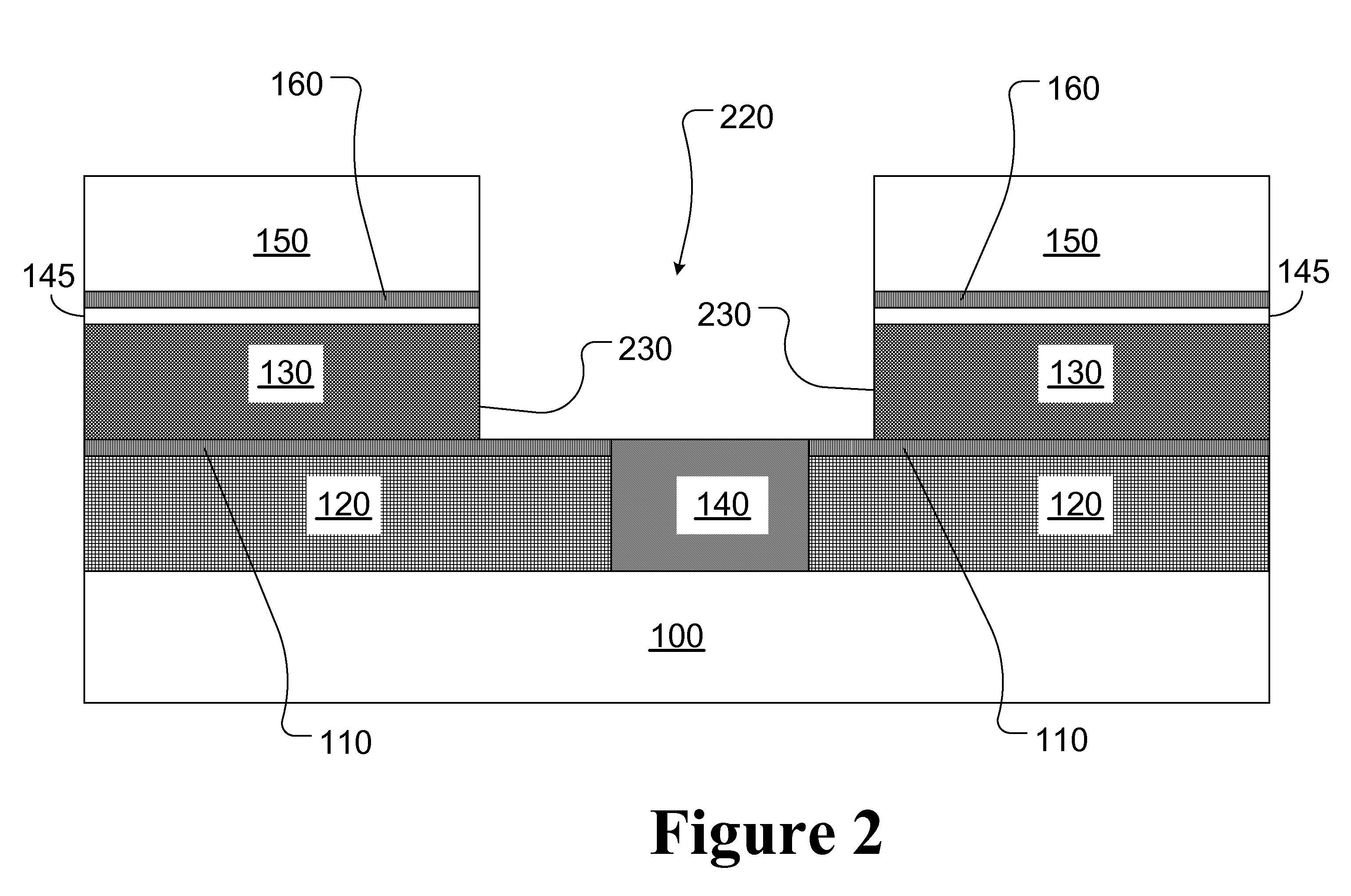
[0013] In still another aspect of the present invention, a structure in a semiconductor device useful in determining an endpoint in a chemical-mechanical polishing process is provided. The structure comprises a dielectric layer, an anti-reflective coating, and a metal layer. The dielectric layer has an opening extending therein. The anti-reflective coating extends over at least a portion of the first dielectric layer. The metal layer extends over at least a portion of the anti-reflective coating and within the opening.
[0014] In yet another aspect of the present invention, a structure in a semiconductor device useful in determining an endpoint in a chemical-mechanical polishing process is provided. The structure comprises a dielectric layer and a metal layer. The dielectric layer has an o

Problems solved by technology

A typical objective is to remove the metal process layer down to the upper surface of the insulative layer, but this is not always the case.
Excessive overpolishing increases the chances of damaging the surface of the polished layer, uses more of the consumable slurry and pad than may be necessary, and reduces the production rate of the CMP equipment.
Also, variations in material thickness may cause the endpoint to change.
First, where the underlying layer has a reflectivity similar to that of the copper layer, the change in reflectivity may not be sufficient to trigger the endpoint detection.
A second problem with optical reflection techniques may arise when the coverage of the copper layer is high.
This problem is exacerbated where the underlying layer has a reflectivity that is not substantially different from that of the copper layer.

Method used


Image

  • Method And Apparatus For Detecting The Endpoint Of A Chemical-Mechanical Polishing Operation
  • Method And Apparatus For Detecting The Endpoint Of A Chemical-Mechanical Polishing Operation
  • Method And Apparatus For Detecting The Endpoint Of A Chemical-Mechanical Polishing Operation

Examples


Embodiment Construction

[0022] Illustrative embodiments of the invention are described below. In the interest of clarity, not all features of an actual implementation are described in this specification. It will be appreciated that in the development of any such actual embodiment, numerous implementation-specific decisions must be made to achieve the developers' specific goals, such as compliance with system-related and business-related constraints, that will vary from one implementation to another. Moreover, it will be appreciated that such a development effort, even if complex and time-consuming, would be a routine undertaking for those of ordinary skill in the art having the benefit of this disclosure.

[0023] The present invention will now be described with reference to FIGS. 1-10. In general, the present invention is directed to a method and apparatus for controlling a CMP process used in the formation of a semiconductor device. As will be readily apparent to those skilled in the art upon a complete re...


PUM


Abstract

A structure in a semiconductor device useful in determining an endpoint in a chemical-mechanical polishing process is provided. The structure comprises a dielectric layer, an anti-reflective coating, and a metal layer. The dielectric layer has an opening extending therein. The anti-reflective coating extends over at least a portion of the first dielectric layer. The metal layer extends over at least a portion of the anti-reflective coating and within the opening. Thus, during the CMP process, the metal layer is removed, exposing the anti-reflective coating but leaving the metal layer in the opening to form a metal interconnect.

Description

BACKGROUND OF THE INVENTION [0001] 1. Field of the Invention [0002] This invention generally pertains to semiconductor processing, and, more particularly, to polishing process layers formed above a semiconducting substrate. [0003] 2. Description of the Related Art [0004] The manufacture of semiconductor devices generally involves the formation of various process layers, selective removal or patterning of portions of those layers, and deposition of additional process layers above the surface of a semiconducting substrate. The substrate and the deposited layers are collectively called a “wafer.” This process continues until a semiconductor device is completely constructed. The process layers may include, by way of example, insulation layers, gate oxide layers, conductive layers, and layers of metal or glass, etc. It is generally desirable in certain steps of the wafer fabrication process that the uppermost surface of the process layers be approximately planar, i.e., flat, for the depo...

Claims


Application Information

Patent Timeline
IPC IPC(8): H01L21/66H01L23/58
CPCB24B37/013H01L21/7684H01L21/76883H01L22/26H01L2924/0002H01L2223/54453H01L23/544H01L2924/00
Inventor MAUERSBERGER, FRANKBECKAGE, PETER J.BESSER, PAUL R.HAUSE, FREDERICK N.RYAN, ERROL TODDBRENNAN, WILLIAM S.JACOPONI, JOHN A.
Owner ADVANCED MICRO DEVICES INC
Learn More