Surface treatments for underfill control

a surface treatment and control technology, applied in the direction of semiconductor devices, electrical equipment, basic electric elements, etc., can solve the problems of reducing the overall module life or seriously degrading performance, bleedout of underfill, and failure of solvent fatigue, so as to reduce or eliminate the bleedout of underfill material and reduce wettability

Inactive Publication Date: 2007-05-03
IBM CORP
View PDF6 Cites 22 Cited by
  • Summary
  • Abstract
  • Description
  • Claims
  • Application Information

AI Technical Summary

Benefits of technology

[0008] The present invention discloses methods to reduce or eliminate the bleed out of underfill material. Surface treatments to selective areas on the chip carrier substrate surface create a non-wettable surface or a reduced wettability surface in the areas where the underfill should not flow. This provides control of the bleed out of the underfill such that the underfill does not bleed or “creep” into areas where it is not wanted, such as under peripheral chip components.

Problems solved by technology

A problem with the chip join of silicon chips on ceramic chip carriers has been solder fatigue fails as a result of the coefficient of thermal expansion “CTE” mismatch between silicon (3 ppm / ° C.) and alumina (6-8 ppm / ° C.).
Despite these benefits, the application of underfill material has created problems which can reduce overall module life or seriously degrade performance.
One such problem occurs if neighboring components are contacted by the spreading or advancing underfill material during its application to the chip carrier, or subsequent processing.
Underfill bleedout is a particular problem in the Bond, Assemble and Test (BAT) manufacturing sectors where chips and peripheral chip devices are attached to the substrate.
Underfill seepage into IDC joint areas, especially partial or incomplete encapsulation, can result in early failure of the IDC joints.
If they are encapsulated with underfill and are subjected to a subsequent second level reflow, melting of the solder in the components may occur.
The volume expansion of the encapsulated solder during melting could cause problems, including extrusion of the solder material, resulting in shorting, etc.

Method used


Image

  • Surface treatments for underfill control
  • Surface treatments for underfill control

Examples


Embodiment Construction

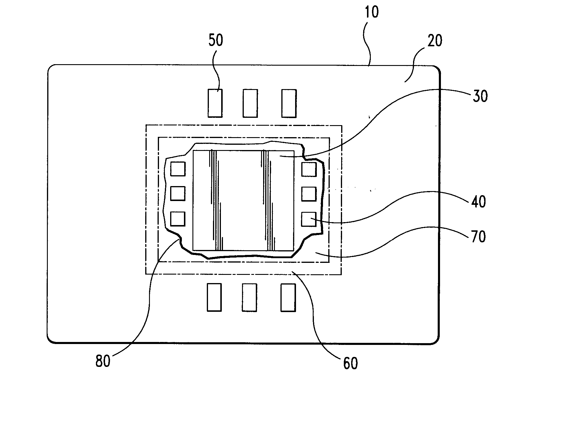
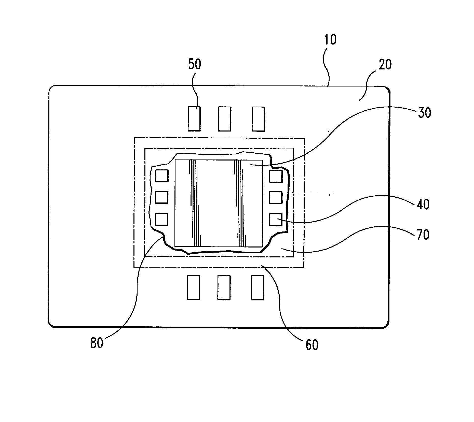
[0017] The purposes of the present invention have been achieved by providing methods of treating a chip carrier ceramic surface to change the wetting characteristics of the surface. The underfill will be less wettable to the treated surface, and this will reduce the bleed out of the underfill and prevent or mitigate the flow of the underfill encapsulation into undesired areas such as underneath the surface mount components. Preferred methods of treating the surface include media blasting or chemical exposure.

[0018] Referring to FIG. 1 there is shown a ceramic chip carrier substrate 10 having a top surface 20 to which a semiconductor chip 30, capacitors 40 and surface mount IDC components 50. There is an area 60 depicted where the surface is intentionally treated by media blasting, grit blasting, or chemical means, to prevent underfill bleed out. The surface treatment creates two regions on the top surface 20. One is the region 70 where the semiconductor chip and C4 capacitors are a...


PUM


Abstract

Methods to reduce or eliminate the bleed out of underfill material. Surface treatments to selective areas on a chip carrier substrate surface create a non-wettable surface or a reduced wettability surface in the areas where the underfill should not flow. The substrate surface is subjected to surface treatments such as media blasting or chemical exposure which will roughen the exposed surface.

Description

BACKGROUND OF THE INVENTION [0001] The present invention is directed to interconnect structures for joining an integrated semiconductor device to a chip carrier substrate and particularly to the controlled application of encapsulant material to the semiconductor device connections to enhance the fatigue life of the semiconductor device solder connections. [0002] Controlled Collapse Chip Connections (C4) or flip-chip technology has been successfully employed for interconnecting high I / O (input / output) count and area array solder bumps on silicon semiconductor devices or “chips” to ceramic chip carriers or substrates. Alumina and glass ceramic substrates are common examples of ceramic chip carriers. A problem with the chip join of silicon chips on ceramic chip carriers has been solder fatigue fails as a result of the coefficient of thermal expansion “CTE” mismatch between silicon (3 ppm / ° C.) and alumina (6-8 ppm / ° C.). The typical solution to this problem has been to encapsulate all ...

Claims


Application Information

Patent Timeline
Patent Type & Authority Applications(United States)
IPC IPC(8): H01L21/00
CPCH01L21/563H01L2224/73203H01L2924/01078H01L2924/09701H01L2924/10253H01L2924/00
Inventor FAROOQ, MUKTALOMBARDI, THOMASNADEAU FILTREAU, JULIEBRADLEY, SCOTTBLAIS, CLAUDEINDYK, RICHARD F.
Owner IBM CORP
Why Eureka
Try Eureka