Semiconductor device

a technology of semiconductor devices and semiconductors, applied in semiconductor devices, semiconductor/solid-state device details, electrical apparatus, etc., can solve the problems of lowering moisture resistance, raising equipment costs and manufacturing costs, and achieve high toughness, high efficiency, and high efficiency.

Inactive Publication Date: 2007-05-03
NEC ELECTRONICS CORP
View PDF3 Cites 10 Cited by
  • Summary
  • Abstract
  • Description
  • Claims
  • Application Information

AI Technical Summary

Benefits of technology

[0008] As means for preventing the cracking of the resin substrate or the semiconductor element, the tape (release film), mentioned above, may be used. However, in such case, it is necessary to provide the resin sealing device, having a function of providing the tape to a space between the resin substrate and the metal mold, thus raising the equipment cost and the manufacturing cost.
[0009] Hence, it is felt to be necessary to provide simplified means for increasing the toughness of the semiconductor device itself for preventing the semiconductor device from becoming deformed at the time of resin sealing.
[0011] An epoxy resin, used as a material of the resin substrate, for example, has an elastic bending modulus which is lowered significantly at a temperature of 150° C. or higher. At 180° C., which is the heating temperature for transfer molding, the elastic bending modulus is at most one-half of that at 25° C. On the other hand, the Barcol hardness of the epoxy resin commences to be lowered at 100 to 150° C., as does the modulus of elasticity, with the hardness at 180° C. being one-half of that at 25° C. or even lower. Conversely, the modulus of elasticity as well as the hardness of metals, such as gold, nickel or copper, making up the conductor patterns, formed on the resin substrate, at 180° C., is scarcely changed from those at 25° C. Thus, the present invention provides a semiconductor device in which a larger proportion of the surface of the resin substrate encapsulated with a resin is covered up with conductor patterns (metallization) for preventing the resin substrate from becoming deformed under the heating and the pressurization at the time of resin encapsulation for thereby raising the toughness of the semiconductor device at the time of the heating and the pressurization.
[0014] According to the present invention, the proportion of the conductors (metallization) in a contact area between the resin substrate and the encapsulating resin is high so that high toughness may be conferred on the resin substrate. Consequently, the resin substrate is not liable to be deformed on contact with the encapsulating resin at e.g. approximately 180° C. at the time of resin encapsulation. Moreover, since the exposed area of the resin substrate is small, that is, the gap between the neighboring conductor patterns is small, the sealing pressure applied to the softened resin substrate from the encapsulating resin acts on only a limited area, thus suppressing the entire resin substrate, inclusive of the conductor patterns, from becoming deformed. In addition, even in such a case where resin encapsulation is made at a lower temperature not higher than 150° C., it becomes possible to suppress the entire resin substrate inclusive of the conductor patterns from becoming warped due to difference between the thermal distortion between the encapsulating resin and the resin substrate occurring at the time of molding of the encapsulating resin and that occurring at the time of cooling. This prevents the resin substrate and the semiconductor element from cracking.
[0015] Moreover, according to the present invention, since the resin substrate may be prevented from becoming deformed, based on the constitution of the semiconductor substrate itself, it becomes unnecessary to provide a deformation preventive tape between the metal mold and the semiconductor device at the time of resin encapsulation. The result is that the process step and a mechanical component for supplying the tape may be dispensed with, thereby saving production costs and equipment cost. In addition, according to the present invention, since it is sufficient to change the pattern shape of the conductor patterns formed by etching or plating, depending on the particular designing, it becomes possible, by highly simplified means, to prevent the resin substrate from being deformed. Furthermore, the mounting performance of the semiconductor devices may be improved by suppressing the deformation of the semiconductor device.

Problems solved by technology

This high temperature and the high pressure deform the resin substrate to give rise to cracking in the semiconductor element and in the surface of the resin substrate surface carrying the semiconductor element.
Such cracking in the semiconductor element or in the resin substrate tends to raise problems such as lowered moisture-proofness.
However, in such case, it is necessary to provide the resin sealing device, having a function of providing the tape to a space between the resin substrate and the metal mold, thus raising the equipment cost and the manufacturing cost.

Method used


Image

  • Semiconductor device
  • Semiconductor device
  • Semiconductor device

Examples


example

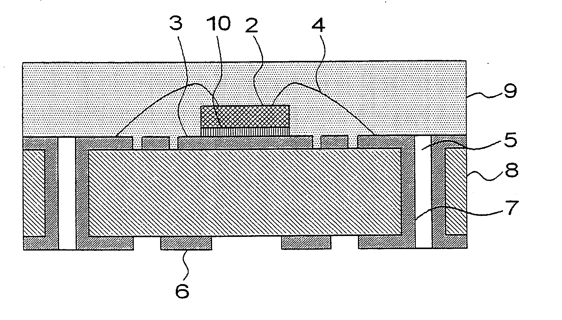
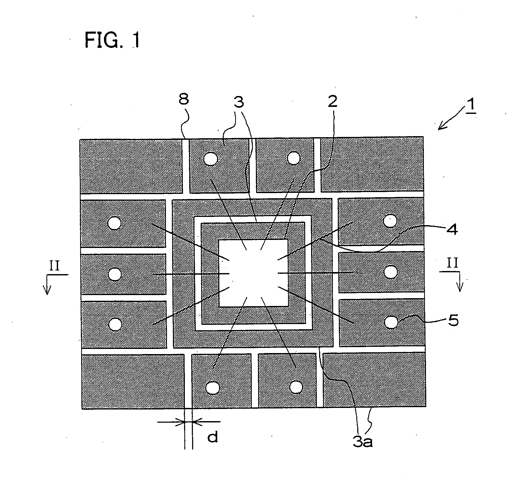
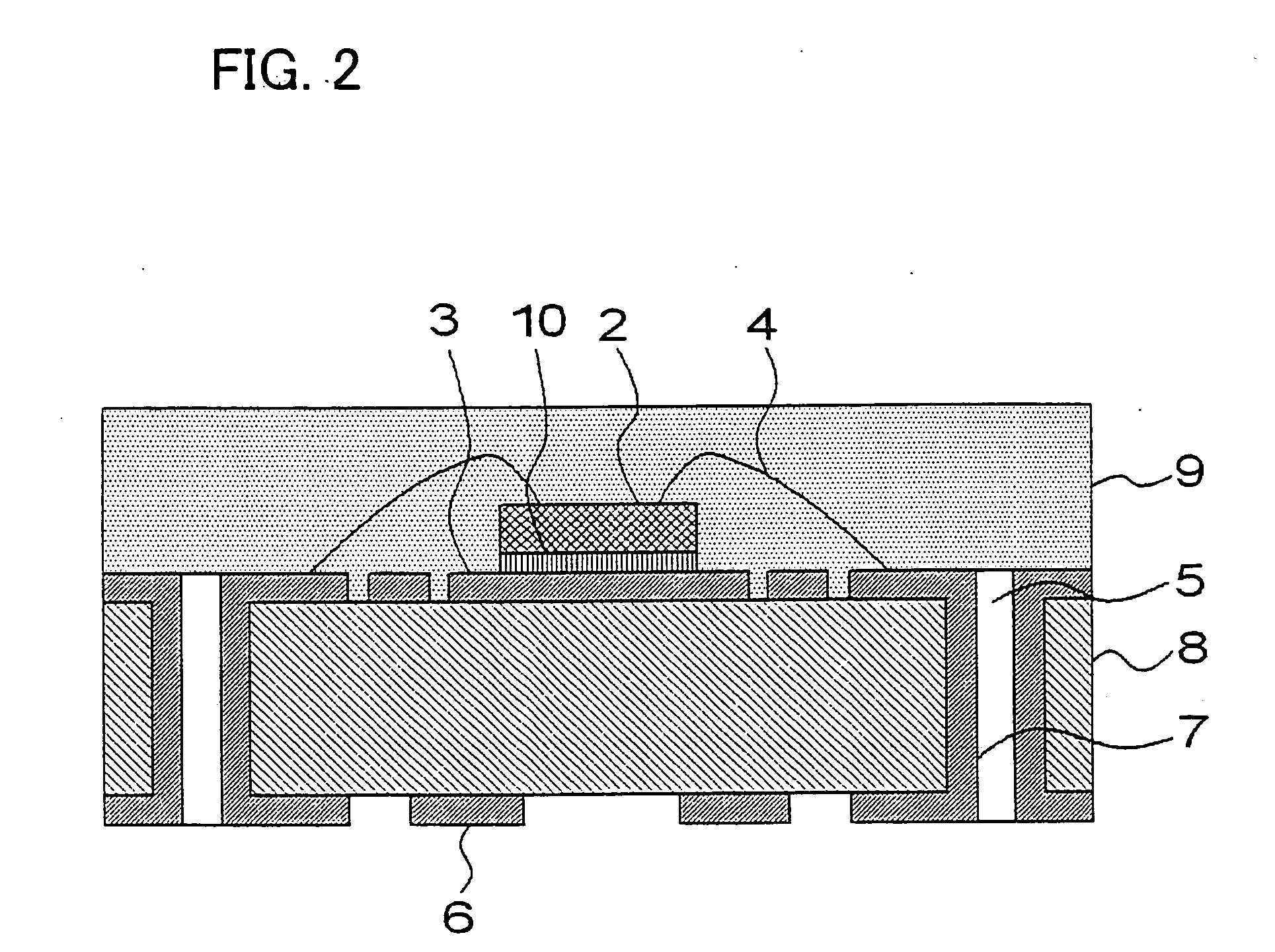
[0032] Samples of the semiconductor devices 1, having different distances d between neighboring conductor patterns of 0.075 mm, 0.10 mm, 0.15 mm, 0.20 mm, 0.25 mm, 0.30 mm, 0.35 mm and 0.375 mm, as shown in FIG. 5, were prepared and checked as to occurrence of cracking at the time of resin encapsulation in each sample of the semiconductor devices 1. The conductor patters are designed to arrange a central square pattern, corner dummy patterns 3a of elongated squares, two squares (each with a through-hole) on upper side and lower side of the figure, respectively, and three elongated patterns (each with a though-hole) on left side and right side, respectively. On a resin substrate 8 of glass epoxy, 110 μm thick, conductor patterns 3, 6, formed of copper, nickel and gold layers, were formed, and a semiconductor element 2 was mounted on an upper conductor patterns 3 (i.e., on the central pattern), using an adhesive 10, containing silver powders. The conductor patterns 3, 6 were formed of...


PUM


Abstract

In a semiconductor device, a occupation ratio of the surface of a resin substrate encapsulated with resin by conductor patterns provided on the same surface is set so as to be 70% or higher in order to raise the toughness of the resin substrate during heating and pressurization. Preferably, the distance between conductor patterns is set so as to be 0.15 mm or less. The resin substrate may be prevented from becoming deformed, that is, a semiconductor device in which cracking in a resin substrate, at the time of resin encapsulation, may be prohibited in a simplified manner from occurrence.

Description

FIELD OF THE INVENTION [0001] This invention relates to a semiconductor device including a resin-encapsulated semiconductor element. BACKGROUND OF THE INVENTION [0002] Nowadays, a semiconductor device, in which a semiconductor element, a passive element and so forth are mounted on a semiconductor substrate, and in which electrical interconnection is formed by film-shaped conductor patterns or fine metal wires, is in use in, for example, a mobile communication terminal. In such semiconductor device, the semiconductor element or the like, on the substrate, is encapsulated with a resin for assuring protection against chemical or physical actions. [0003]FIGS. 7 and 8 are schematic views of a semiconductor device according to the related art in which a resin substrate carrying a semiconductor element thereon has its surface encapsulated with a resin. More specifically, FIG. 7 depicts a top plan view of the semiconductor device when viewed from the side of the surface of the resin substra...

Claims


Application Information

Patent Timeline
IPC IPC(8): H01L23/48H01L23/52H01L29/40
CPCH01L23/3121H01L23/49838H01L24/45H01L24/49H01L2224/45144H01L2224/48091H01L2224/49171H01L2924/01004H01L2924/01013H01L2924/01028H01L2924/01029H01L2924/01033H01L2924/01047H01L2924/01078H01L2924/01079H01L2924/00014H01L24/48H01L2924/01006H01L2924/014H01L2224/32225H01L2224/48227H01L2224/73265H01L2924/181H01L2924/00012H01L2924/00H01L23/02
Inventor MURAI, NOBUHIRO
Owner NEC ELECTRONICS CORP
Why Eureka
Try Eureka