Spin-transfer switching magnetic elements using ferrimagnets and magnetic memories using the magnetic elements
a technology of ferrimagnets and magnetic elements, applied in the field of magnetic memory systems, can solve the problems of increasing power consumption, adversely affecting the utility and reliability of such conventional magnetic elements, and conventional magnetic elements b>10/b>
- Summary
- Abstract
- Description
- Claims
- Application Information
AI Technical Summary
Benefits of technology
Problems solved by technology
Method used
Image
Examples
first embodiment
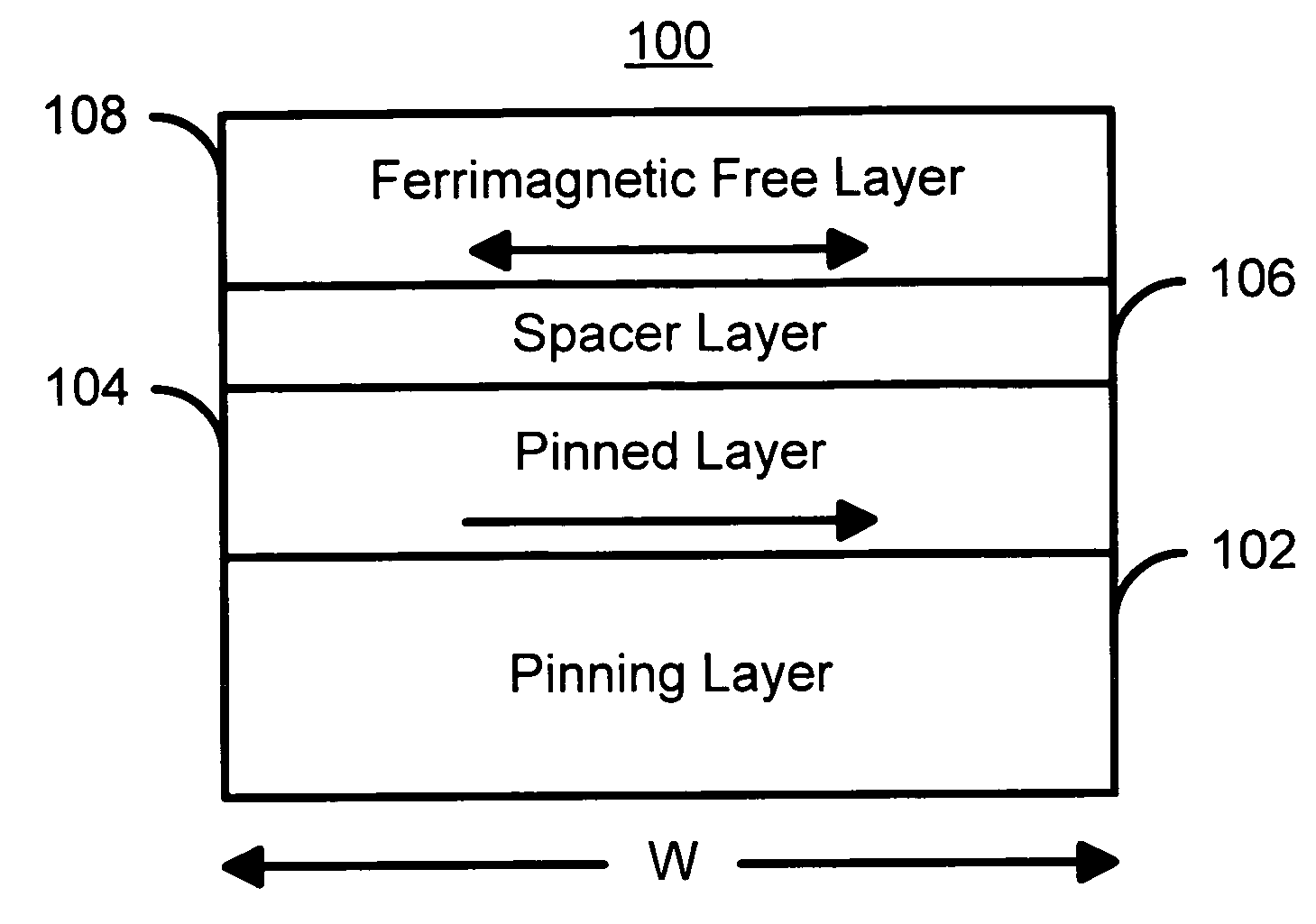
[0024]FIG. 3 is a diagram of a magnetic element 100 in accordance with the present invention and which can be written using spin transfer. The magnetic element 100 includes a pinning layer 102 that is preferably an AFM layer, pinned layer 104, a spacer layer 106, and a free layer 108 that is ferrimagnetic. In an alternate embodiment, the pinning layer 102 may be omitted in favor of another mechanism for pinning the magnetizations of the pinned layer 104. In a preferred embodiment, the AFM layer 102 includes materials such as PtMn and IrMn which have a high blocking temperature, above two hundred degrees Celsius. In addition, one or more seed layers (not shown) may be used to provide a desired texture of the AFM layer 102. The pinned layer 104 may be a simple layer, for example composed of a ferromagnetic alloy including Co, Fe, or Ni. Additives such as B and / or Ta may optionally be added to modify the structure of the pinned layer 104. The pinned layer 104 may also be a synthetic pi...
second embodiment
[0043]FIG. 5 is a diagram of a magnetic element 150 in accordance with the present invention and which can be written using spin transfer. Portions of the magnetic element 150 are analogous to the magnetic element 100. However, the magnetic element 150 is a dual structure including two pinned and two spacer layers. The magnetic element 150 includes a first pinning layer 152 that is preferably an AFM layer, a first pinned layer 154, a first spacer layer 156, a free layer 158 that is ferrimagnetic, a second spacer layer 160, a second pinned layer 162, and a second pinning layer 164. In an alternate embodiment, one or more of the pinning layers 152 and 164 may be omitted in favor of another mechanism for pinning the magnetizations of the pinned layers 154 and 162. In a preferred embodiment, the AFM layers 152 and 164 include materials such as PtMn and IrMn which have a high blocking temperature. In addition, one or more seed layers (not shown) may be used to provide a desired texture o...
PUM
 Abstract
Description
Claims
Application Information
 - R&D
- Intellectual Property
- Life Sciences
- Materials
- Tech Scout
- Unparalleled Data Quality
- Higher Quality Content
- 60% Fewer Hallucinations
Browse by: Latest US Patents, China's latest patents, Technical Efficacy Thesaurus, Application Domain, Technology Topic, Popular Technical Reports.
© 2025 PatSnap. All rights reserved.Legal|Privacy policy|Modern Slavery Act Transparency Statement|Sitemap|About US| Contact US: help@patsnap.com


