Development apparatus and development method

a technology of development apparatus and development method, which is applied in the direction of printers, instruments, photosensitive materials, etc., can solve the problems of reducing the uniformity of the pattern line width that is finally formed in the wafer plane, and achieves the effect of high in-plane uniformity

Inactive Publication Date: 2007-03-22
TOKYO ELECTRON LTD
View PDF3 Cites 14 Cited by
  • Summary
  • Abstract
  • Description
  • Claims
  • Application Information

AI Technical Summary

Benefits of technology

[0011] It is an object of the present invention to provide a development apparatus and a development method which can form a liquid film of a developer having a thickness with high in-plane uniformity on a substrate while suppressing generation of a liquid flow in the liquid film of the developer when supplying the developer onto a coating film on the substrate.
[0027] According to the present invention, since there is adopted a structure in which the liquid flow suppressing member including the mesh having the hydrophilic properties with respect to the developer is provided at a height position where this member comes into contact with a surface of the developer supplied to the substrate or it is immersed in the liquid, it is possible to suppress generation of a liquid flow phenomenon (flowage) in the liquid film of the developer existing in a gap between the substrate and the liquid flow suppressing member. Moreover, since provision of the hydrophilic properties can improve wettability of the developer and the developer can be thereby uniformly transmitted within a plane of the liquid flow suppressing member, the liquid film of the developer having a uniform thickness can be formed on the surface of the substrate. As a result, a mask pattern having high in-plane uniformity with respect to a line width can be formed on the surface of the substrate after development.

Problems solved by technology

As a result, since progress of a development reaction becomes non-homogeneous in the wafer plane and unevenness is produced in a resist resolution, there is a risk of a reduction in uniformity of a pattern line width which is finally formed in the wafer plane.
However, this conventional technique has the following problems.

Method used


Image

  • Development apparatus and development method
  • Development apparatus and development method
  • Development apparatus and development method

Examples


Embodiment Construction

[0050] Preferred embodiments according to the present invention will now be described hereinafter with reference to the accompanying drawings.

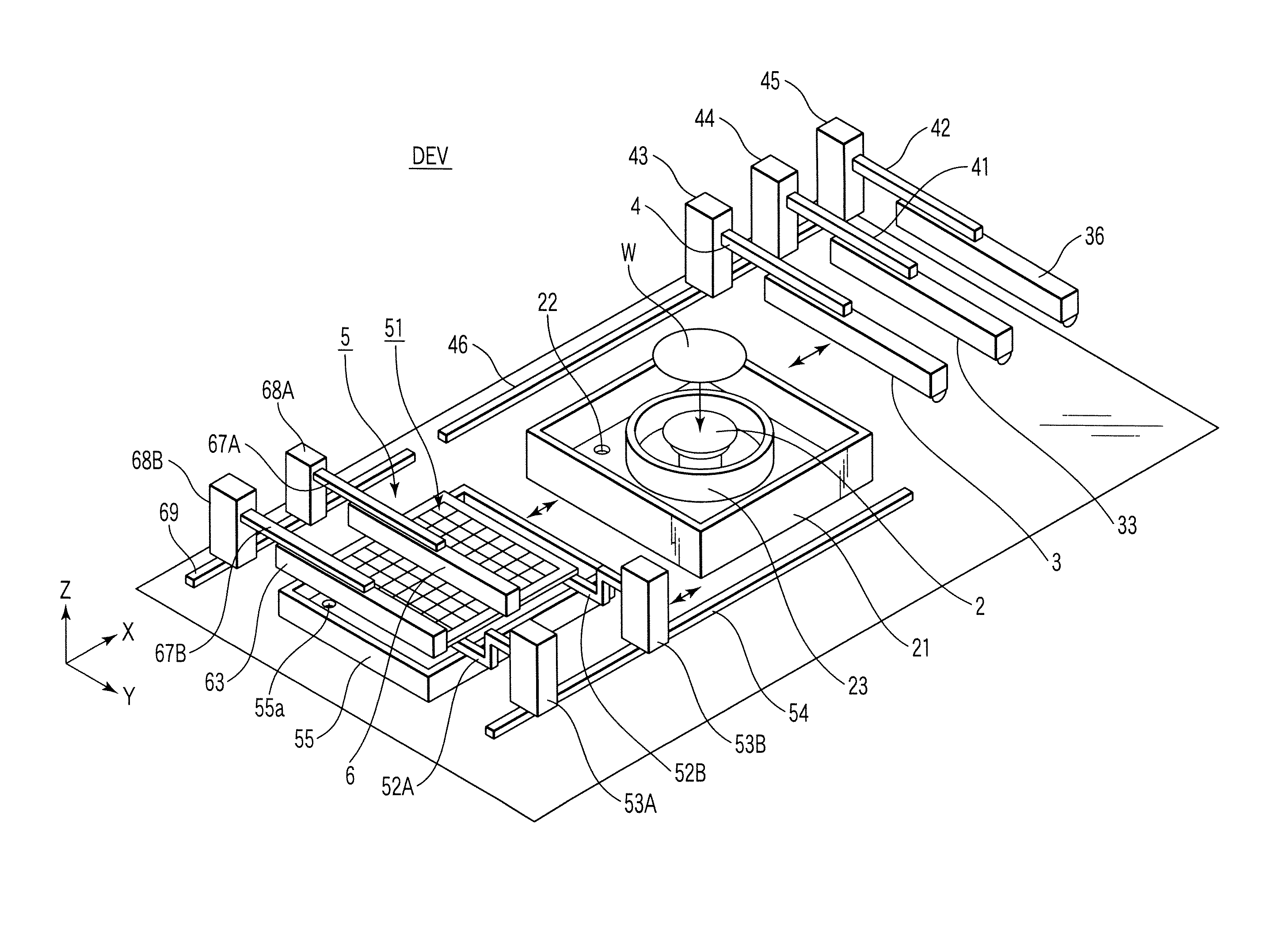
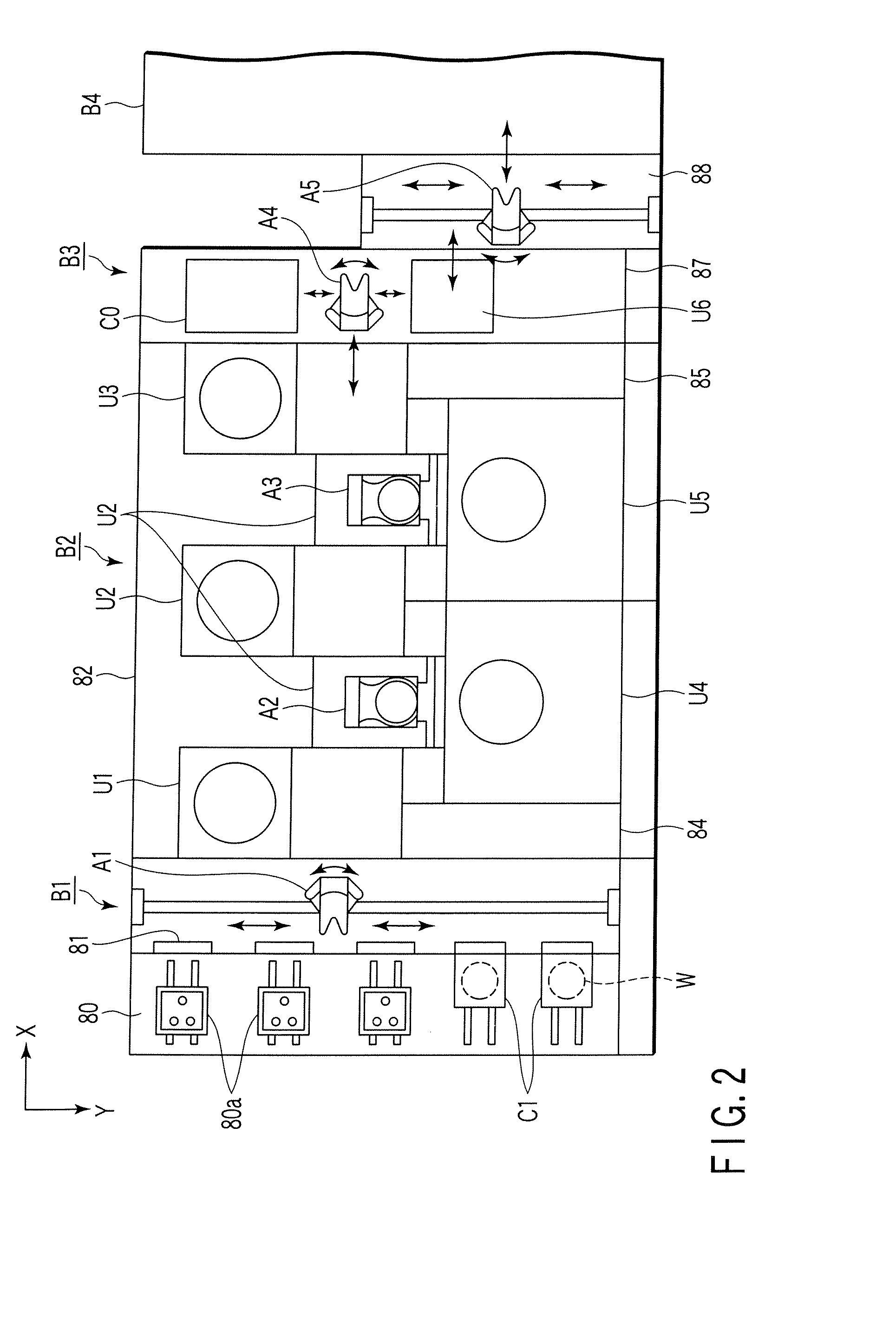
[0051] A development apparatus according to the present invention is incorporated as a development unit DEV in a coating / development apparatus shown in FIGS. 2 and 3. Reference character B1 in the drawing denotes a carrier mount portion which carries in and out a carrier C in which, e.g., 13 semiconductor wafers W are accommodated. The carrier mount portion B1 is provided with a carrier station 8 including a mount portion 80 in which the plurality of carriers C can be mounted, opening / closing portions 81 provided on a wall surface on a front side as seen from the carrier station 8, and a sub-carriage arm mechanism Al which is used to take out the wafer W from the carrier C through each opening / closing portion 81.

[0052] A processing portion B2 is connected on the innermost side of the carrier mount portion B1 in an X direction, and the proces...


PUM

PropertyMeasurementUnit
contact angleaaaaaaaaaa

Abstract

A development apparatus has a holder which horizontally holds a substrate, a nozzle which supplies a developer to a resist film on the substrate held by the holder, a liquid flow suppressing member whose size in a two-dimensional plane viewing field is equal to or larger than that of the substrate and which has a mesh having many openings and hydrophilic properties with respect to the developer and transmits the developer supplied from the nozzle through the openings of the mesh to form a liquid film of the developer between the mesh and the substrate, and a moving mechanism which movably supports this liquid flow suppressing member, sets the mesh to face the resist film on the substrate and brings the mesh into contact with a surface of the liquid film of the developer or immerges the mesh in the liquid film.

Description

CROSS REFERENCE TO RELATED APPLICATIONS [0001] This is a Continuation Application of PCT Application No. PCT / JP2005 / 008995, filed May 17, 2005, which was published under PCT Article 21(2) in Japanese. [0002] This application is based upon and claims the benefit of priority from prior Japanese Patent Application No. 2004-148115, filed May 18, 2004, the entire contents of which are incorporated herein by reference. BACKGROUND OF THE INVENTION [0003] 1. Field of the Invention [0004] The present invention relates to a development apparatus and a development method which develop a resist coating film subjected pattern exposure. [0005] 2. Description of the Related Art [0006] In a photolithography process for a semiconductor device, a system in which a coating / development apparatus is combined with an exposure device is used. A development nozzle of the coating / development apparatus is provided with a linear discharge opening which is equal to or longer than a diameter of a semiconductor ...

Claims


Application Information

Patent Timeline
Patent Type & Authority Applications(United States)
IPC IPC(8): G03D5/00G03F7/30H01L21/00H01L21/027
CPCH01L21/6715G03F7/3021G03F7/30
Inventor KITAMURA, TETSUYA
Owner TOKYO ELECTRON LTD
Why Eureka
Try Eureka