
Apparatus and methods for packaging antennas with integrated circuit chips for millimeter wave applications

a technology of integrated circuit chips and antenna devices, applied in the direction of resonant antennas, instruments, semiconductor/solid-state device details, etc., can solve the problems of increasing the difficulty of manufacturing and assembly of conventional waveguide front-ends, increasing the difficulty of achieving high-performance systems, and increasing the cost of bulky wave guides. achieve the effect of high-integration and high-performan

Active Publication Date: 2007-03-22
GLOBALFOUNDRIES US INC
View PDF1 Cites 142 Cited by
  • Summary
  • Abstract
  • Description
  • Claims
  • Application Information

AI Technical Summary

Benefits of technology

[0006] In general, exemplary embodiments of the invention include apparatus and methods for integrally packaging antennas with semiconductor IC (integrated circuit) chips to provide highly-integrated and high-performance radio/wireless communications systems for millimeter wave applications including, e.g., voice communication, data communication and radar applications. More specifi

Problems solved by technology

For example, MMW radio communication systems are typically built using expensive and bulky wave guides and / or package-level or board-level microstrip structures that provide electrical connections between semiconductor chips (RF integrated circuits) and between semiconductor chips and transmitter or receiver antennas.
As the operating frequency increases, the manufacture and assembly of conventional waveguide front-ends become more difficult.
With increased integration, however, the ability to achieve high performance systems becomes more problematic, especially at millimeter wave frequencies wherein the structure and EM characteristics of the integrated antenna system will determine the achievable performance of the system.
With high-integration designs, design tradeoffs are typically made with respect to antenna performance (e.g., tradeoffs between antenna bandwidth and efficiency).

Method used


Image

  • Apparatus and methods for packaging antennas with integrated circuit chips for millimeter wave applications
  • Apparatus and methods for packaging antennas with integrated circuit chips for millimeter wave applications
  • Apparatus and methods for packaging antennas with integrated circuit chips for millimeter wave applications

Examples


Embodiment Construction

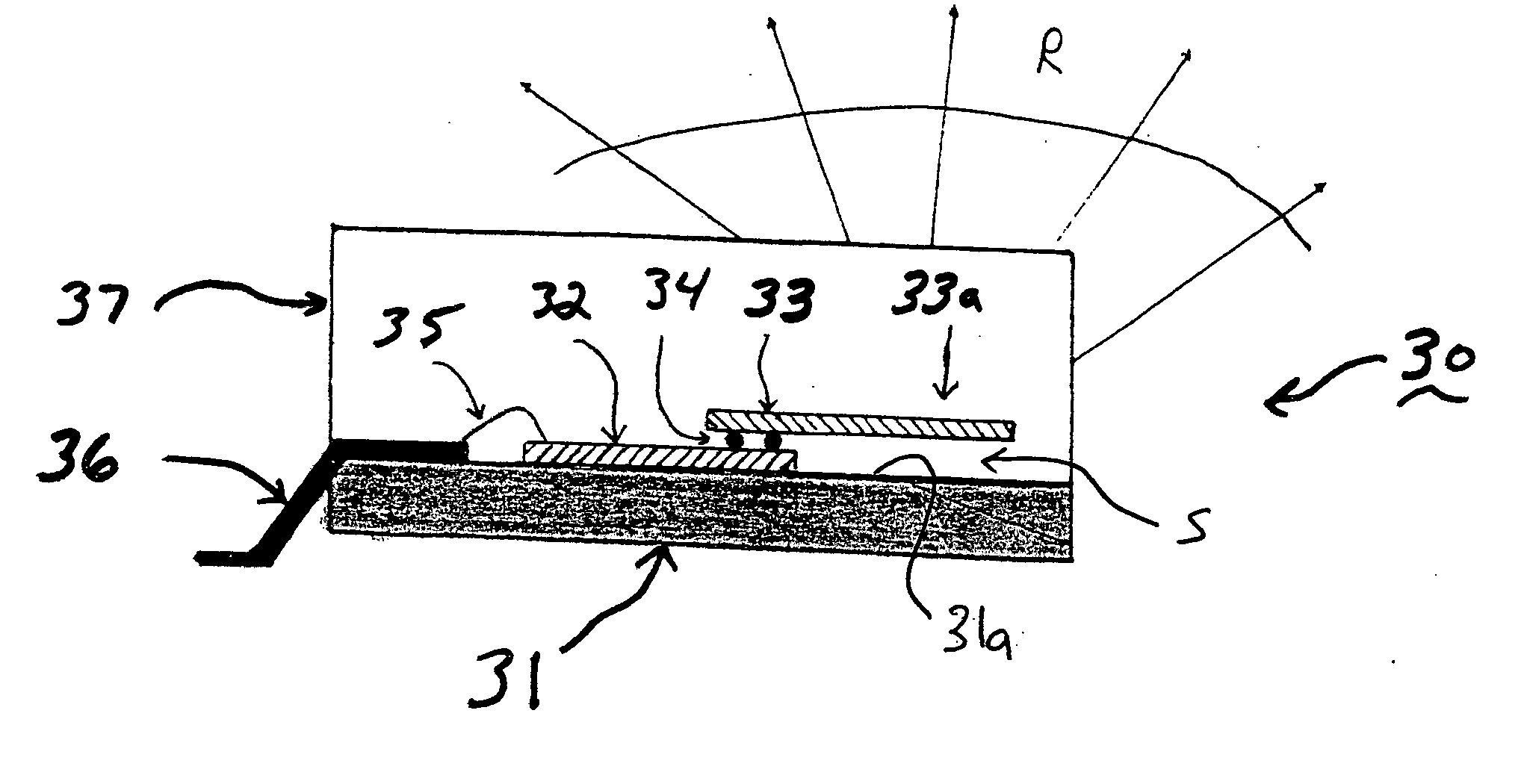
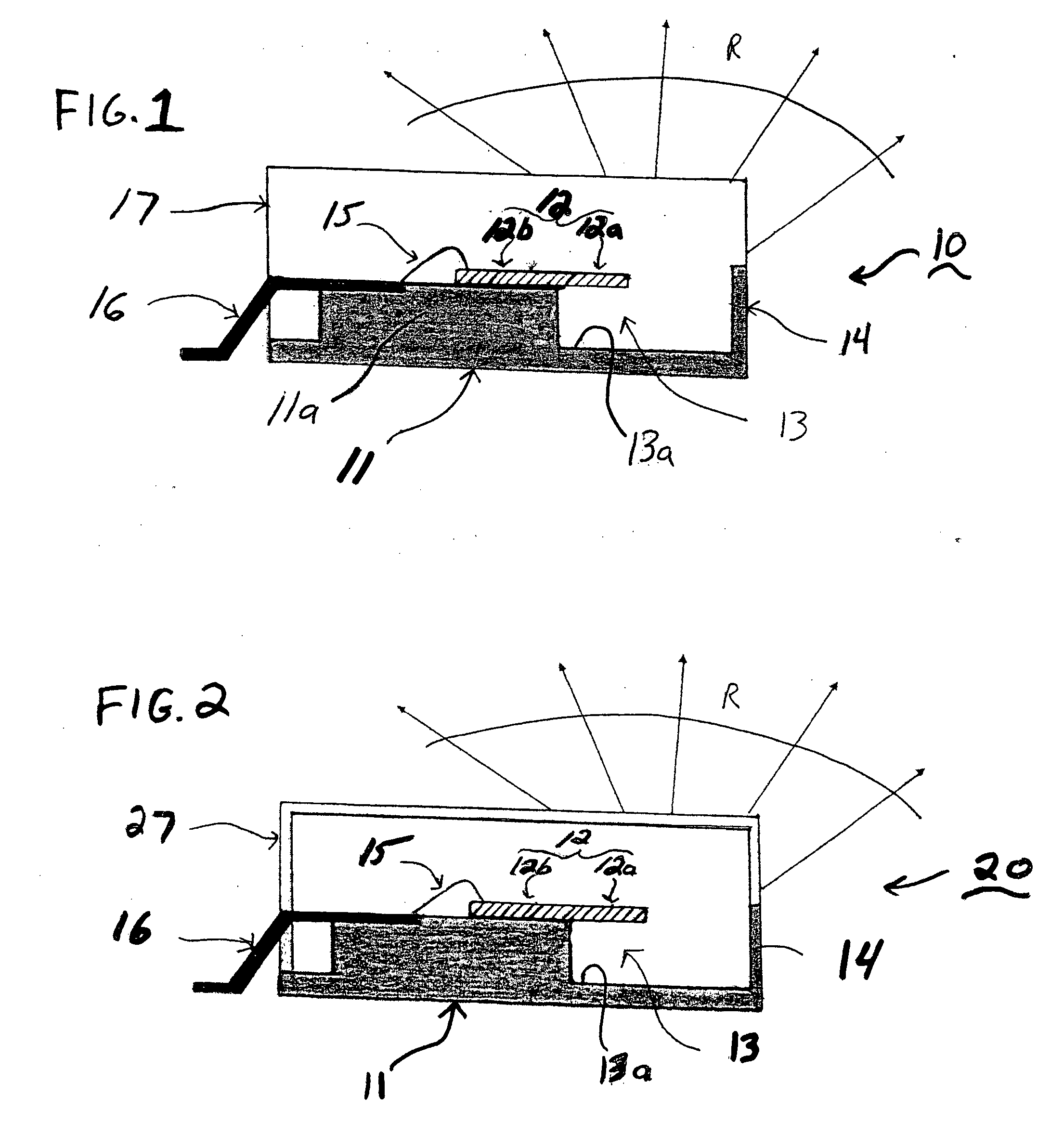
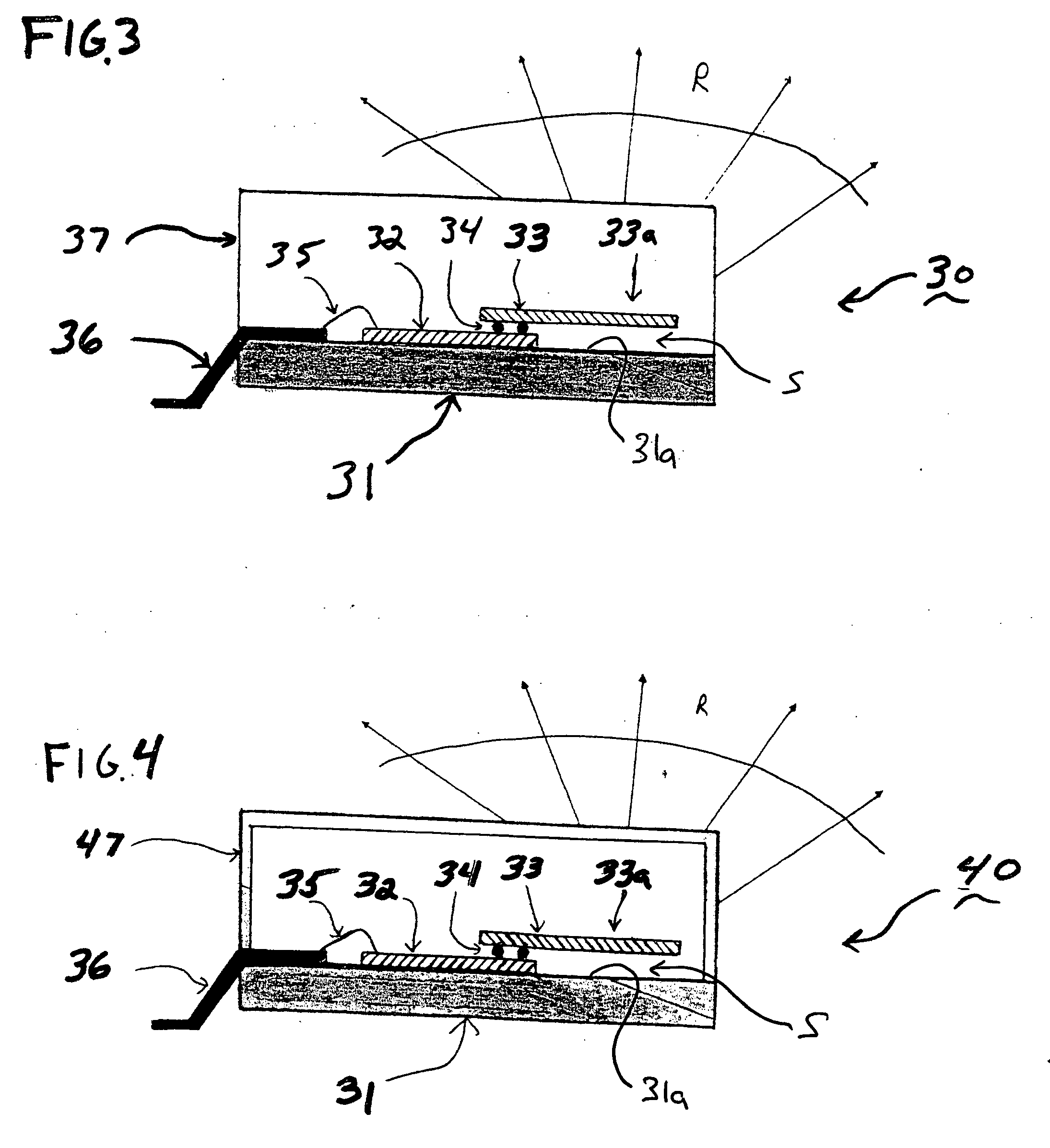
[0025] In general, exemplary embodiments of the invention as described herein include apparatus and methods for integrally packaging antennas with semiconductor IC (integrated circuit) chips to provide highly-integrated and high-performance radio / wireless communications systems for millimeter wave applications including, e.g., voice communication, data communication and radar applications. More specifically, exemplary embodiments of the invention include apparatus and methods for constructing compact wireless communication modules in which antenna systems are integrally packaged with IC chips having integrated receiver / transmitter / transceiver circuits. For example, exemplary embodiments of the invention (such as described below with reference to FIGS. 1-2 and 7-9) include wireless communication modules that include IC chips having on-chip active RF circuits and planar antennas that are integrally formed as part of a BEOL (back-end-of-line) metallization structure of the IC chip. In ...


PUM


Abstract

Apparatus and methods are provided for integrally packaging antennas with semiconductor IC (integrated circuit) chips to provide highly-integrated and high-performance radio / wireless communications systems for millimeter wave applications including, e.g., voice communication, data communication and radar applications. For example, wireless communication modules are constructed with IC chips having receiver / transmitter / transceiver integrated circuits and planar antennas that are integrally constructed from BEOL (back end of line) metallization structures of the IC chip.

Description

TECHNICAL FIELD OF THE INVENTION [0001] The present invention generally relates to apparatus and methods for integrally packaging antenna devices with semiconductor IC (integrated circuit) chips and, in particular, apparatus and methods for packaging IC chips with planar antennas that are integrally constructed from BEOL (back end of line) metallization structures, for example, to thereby form compact integrated radio / wireless communications systems for millimeter wave applications. BACKGROUND [0002] Technological innovations in wireless systems and devices have lead to widespread development of wireless network applications for wireless PAN (personal area network), wireless LAN (local area network), wireless WAN (wide area network), cellular networks, and other types of wireless communication systems. To enable wireless communication between devices in a wireless network, the devices must be equipped with receivers, transmitters, or transceivers, as well as antennas that can effici...

Claims


Application Information

Patent Timeline
IPC IPC(8): G06K19/06H01L23/02H05K1/14
CPCH01L23/4334H01L23/5227H01L2924/12041H01L2924/1423H01L2224/73265H01L2924/014H01L2924/01074H01L2924/01006H01L2924/01005H01L24/49H01L24/48H01L23/66H01L24/73H01L2223/6677H01L2224/16145H01L2224/48227H01L2224/48247H01L2224/49175H01L2224/8592H01L2924/01013H01L2924/01033H01L2924/01082H01L2924/10329H01L2924/3011H01Q3/26H01Q9/16H01Q19/30H01Q23/00H01L2924/00H01L2224/32225H01L2224/48091H01L2924/00014H01L2924/14H01L2924/181H01L2924/30111H01L2924/00012H01L2224/45099H01L2224/45015H01L2924/207
Inventor GAUCHER, BRIAN P.LIU, DUIXIANPFEIFFER, ULLRICH R.ZWICK, THOMAS M.
Owner GLOBALFOUNDRIES US INC
Learn More