
Spin transistor using spin-orbit coupling induced magnetic field

a spin-orbit coupling and magnetic field technology, applied in the direction of magnetic materials, semiconductor devices, magnetic bodies, etc., can solve the problems of difficult to further reduce the power consumption and volume of the mosfet, the gate oxide of the mosfet faces physical limitations, and the probability of loss of spin information of the electron, etc., to achieve a greater spin-orbit coupling effect and very fast electron mobility

Active Publication Date: 2007-03-15
KOREA INST OF SCI & TECH
View PDF5 Cites 27 Cited by
  • Summary
  • Abstract
  • Description
  • Claims
  • Application Information

AI Technical Summary

Benefits of technology

[0010] An object of the present invention is to provide a spin transistor having wide ON / OFF operation margin, allowing a broad process margin for channel length and producing less noise.
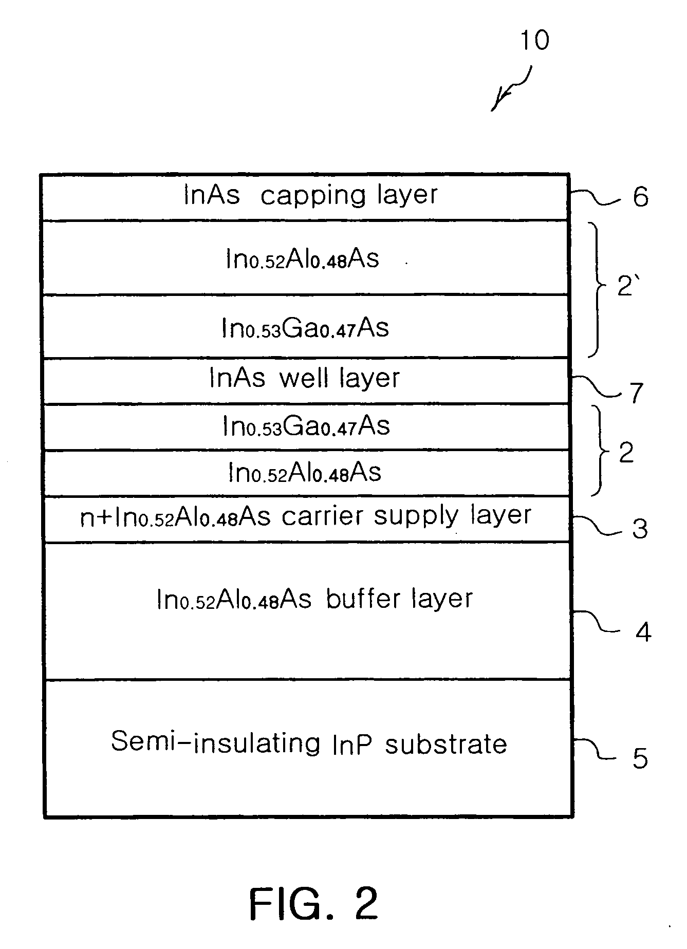
[0013] The channel may be formed as a quantum well layer. Since the quantum well layer has two-dimensional electron gas (2-DEG), mobility of electron is very fast in the well layer and greater spin-orbit coupling effect is occurred. The quantum well layer may be formed of one selected from the group consisting of GaAs, InAs and InGaAs.

Problems solved by technology

For example, it is difficult to further reduce power consumption and volume of the MOSFET.
In addition, the gate oxide of the MOSFET faces physical limitations.
In the conventional spin transistor, spin information of the electron is likely to be lost by stray field generated at the ends of the source and the drain.
The generated stray field shortens an effective distance of spin transfer and makes considerable noise.
However, it is very difficult to precisely adjust an angle of the precession and to accurately form the channel to have a proper length corresponding to the precession angle.
As a result, operating accuracy degrades and a manufacturing process thereof becomes complicated.

Method used


Image

  • Spin transistor using spin-orbit coupling induced magnetic field
  • Spin transistor using spin-orbit coupling induced magnetic field
  • Spin transistor using spin-orbit coupling induced magnetic field

Examples


Embodiment Construction

[0030] Reference will now be made in detail to the preferred embodiments of the present invention, examples of which are illustrated in the accompanying drawings.

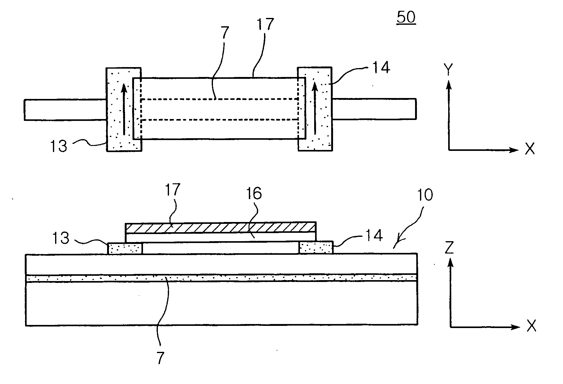
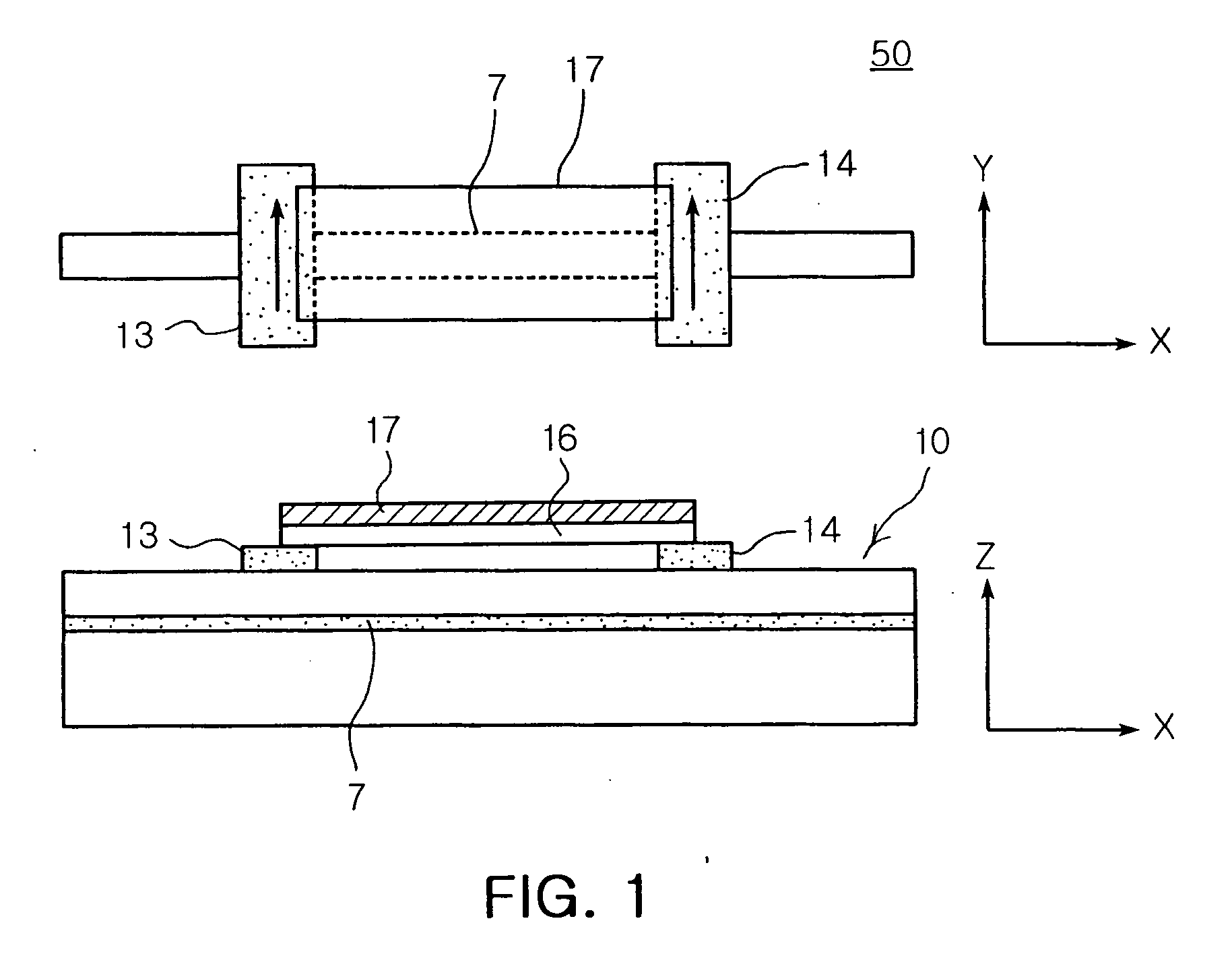
[0031]FIG. 1 is a schematic plan view and a schematic cross-sectional view of a spin transistor according to an embodiment of the present invention.

[0032] Referring to FIG. 1, the spin transistor 50 includes: a substrate 10, a source 13, a drain 14 and a gate 17. The substrate 10 has a quantum well layer 7 as a channel. The source 13, the drain 14 and the gate 17 controlling an ON / OFF operation are formed on the substrate 10. The gate 17 is insulated from the source 13 and the drain 14 by a gate insulating layer 16. The quantum well layer 7 forms a channel of the spin transistor 50. The source 13 and the drain 14 are made of a magnetized ferromagnetic material and have an identical magnetization direction. For example, the source 13 and the drain 14 may be made of ferromagnetic metal such as Fe, Co, Ni, CoFe or NiFe, or f...


PUM


Abstract

A spin transistor having wide ON / OFF operation margin and producing less noise is provided. The spin transistor includes a substrate having a channel, a source, a drain and a gate formed on the substrate. The source and the drain are formed to have magnetization directions perpendicular to the length direction of the channel. The ON / OFF operations of the spin transistor can be controlled by generating a spin-orbit coupling induced magnetic field to have a direction parallel or anti-parallel to the magnetization directions of the source and the drain.

Description

RELATED APPLICATION [0001] The present application is based on, and claims priority from, Korean Application Number 2005-85717, filed Sep. 14, 2005, the disclosure of which is hereby incorporated by reference herein in its entirety. BACKGROUND OF THE INVENTION [0002] 1. Field of the Invention [0003] The present invention relates to a spin transistor using a spin-orbit coupling induced magnetic field, and more particularly, to a spin transistor having a wide ON / OFF operation margin and making less noise that is generated by leakage magnetic field. [0004] 2. Description of the Related Art [0005] A metal oxide silicon field effect transistor (MOSFET) is one of representative elements in a modern integrated circuit technology. The MOSFET is generally included as an essential element for performing ON / OFF switching operation in a memory device such as a flash memory and a DRAM, as well as a logic circuit, ASIC and a microprocessor. Recently, a spin transistor (Spin-FET) is introduced. A ...

Claims


Application Information

Patent Timeline
Patent Type & Authority Applications(United States)
IPC IPC(8): H01L21/8238B82Y10/00H01L21/336H01L29/06H01L29/78H01L29/82
CPCH01F1/404H01F10/193H01L29/772H01L29/66984H01L29/0843H01L21/18
Inventor KOO, HYUN CHEOLHAN, SUK HEEEOM, JONG HWACHANG, JOON YEONYI, HYUN JUNG
Owner KOREA INST OF SCI & TECH
Learn More