Continuous process for manufacturing electrical cables
a manufacturing process and technology for electrical cables, applied in the direction of power cables, cables, insulation conductors/cables, etc., can solve the problems of increasing introducing space and logistic problems, and prolonging the cable manufacturing time, so as to increase the cost of cable production and extend the cable manufacturing time.
- Summary
- Abstract
- Description
- Claims
- Application Information
AI Technical Summary
Benefits of technology
Problems solved by technology
Method used
Image
Examples
example 1
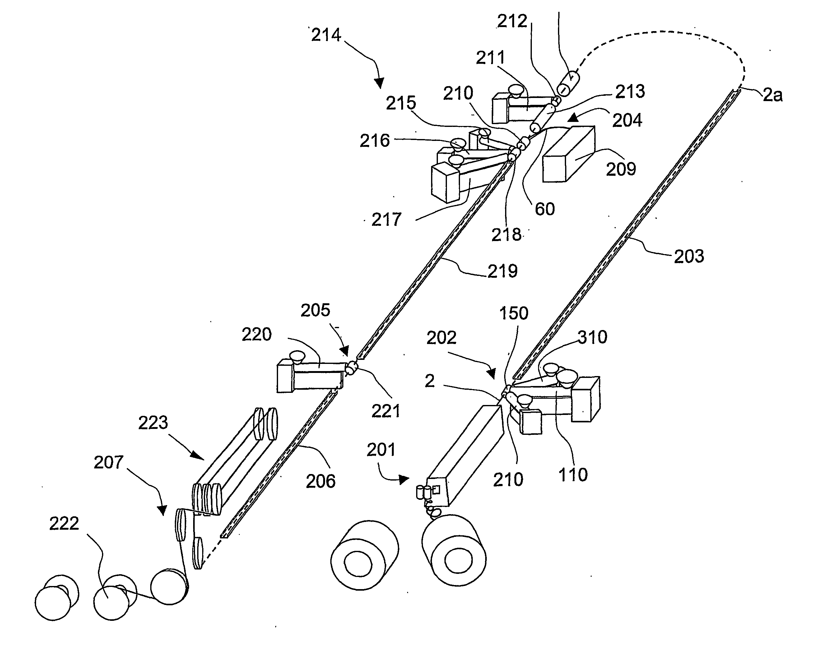
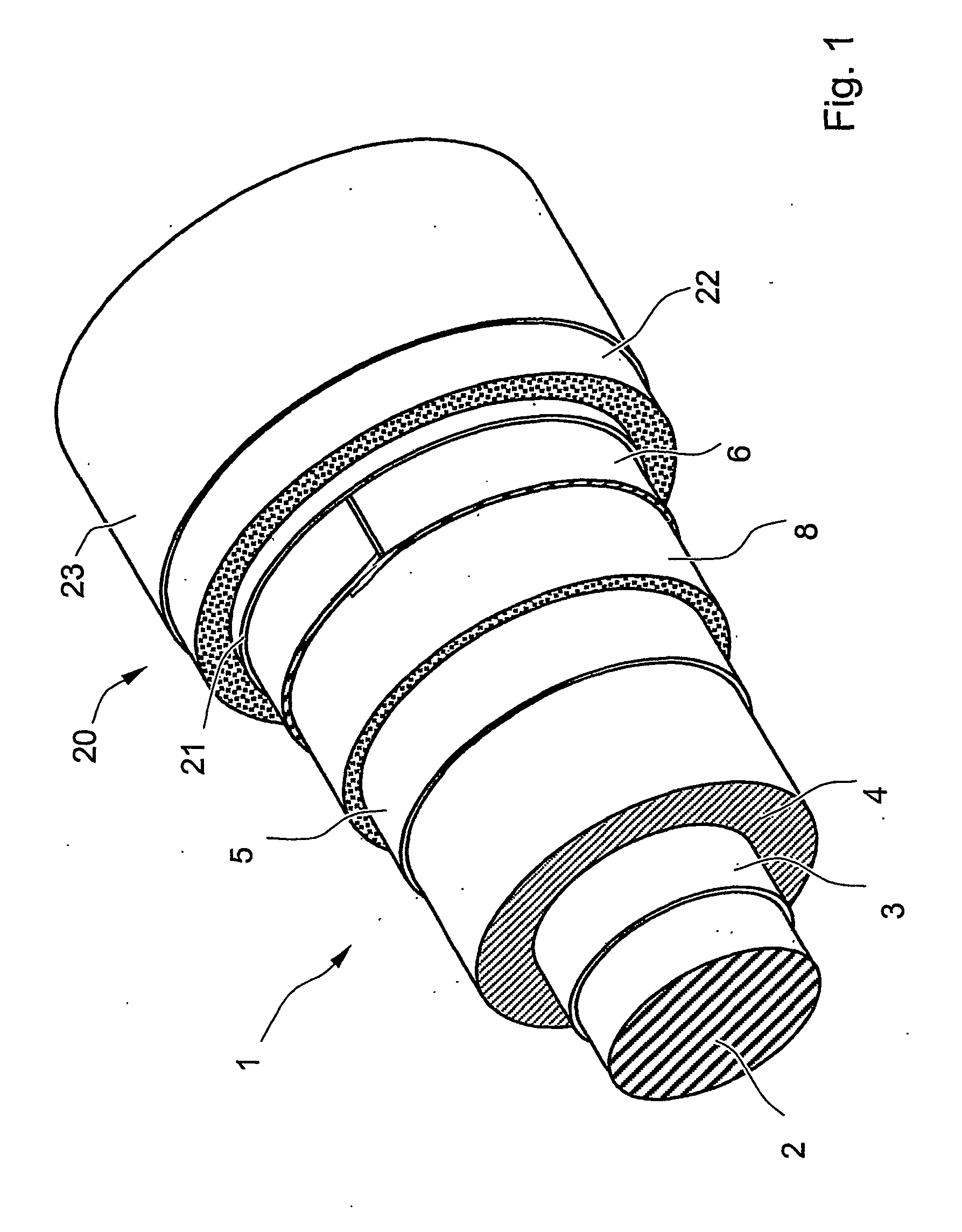
[0174] The following example describes in detail the main steps of the continuous production process of a 150 mm2, 20 kV cable as shown in FIG. 1. The line speed was set at 60 m / min.
a) Cable Core Extrusion
[0175] The cable insulating layer was obtained by feeding directly into the hopper of the extruder 110 a propylene heterophase copolymer having melting point 165° C., melting enthalpy 30 J / g, MFI 0.8 dg / min and flexural modulus 150 MPa (Adflex® Q 200 F—commercial product of Basell).
[0176] Subsequently, the dielectric oil Jarylec® Exp3 (commercial product of Elf Atochem—dibenzyltoluene), previously mixed with the antioxidants, was injected at high pressure into the extruder.
[0177] The extruder 110 had a diameter of 80 mm and a L / D ratio of 25.
[0178] The injection of the dielectric oil was performed—during the extrusion—at about 20 D from the beginning of the screw of the extruder 110 by means of three injections point on the same cross-section at 120° from each other. The diel...
example 2
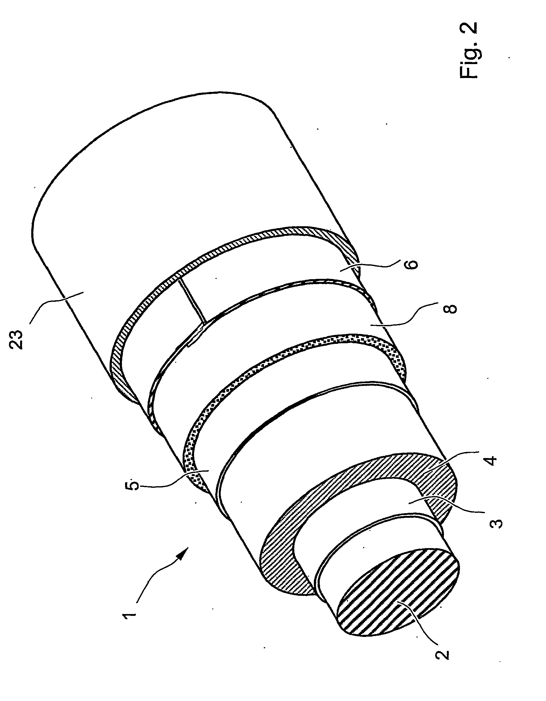
[0224] A continuous process for producing a 50 mm2, 10 kV cable according to FIG. 1 was carried out as described in Example 1. The process line speed was set at 70 m / min.
[0225] The materials used for the constitutive elements of the cable were the same as those disclosed in Example 1.
[0226] The thickness of the insulating layer was of about 2.5 mm, while the thickness of the inner and the outer semiconductive layers was of about 0.2 mm.
[0227] The thickness of the metallic screen was of about 0.2 mm.
[0228] The water blocking semiconductive expanded layer had a thickness of about 0.5 mm and a degree of expansion of 20%.
[0229] The inner polymeric layer 21 was of about 1.0 mm in thickness, while the expanded polymeric layer 22 had a thickness of about 1.5 mm and a degree of expansion of 70%.
[0230] The oversheath 23 was of a thickness of about 0.5 mm.
Thermal Profiles of the Continuous Process
[0231]FIG. 6 shows the thermal profile of the constitutive components of the cable menti...
example 3
[0233] A continuous process for producing a 240 mm2, 30 kV cable according to FIG. 1 was carried out as described in Example 1. The process line speed was set at 50 m / min.
[0234] The materials used for the constitutive elements of the cable were the same as those disclosed in Example 1.
[0235] The thickness of the insulating layer was of about 5.5 mm, while the thickness of the inner and the outer semiconductive layers was of about 0.2 mm.
[0236] The thickness of the metallic screen was of about 0.2 mm.
[0237] The water blocking semiconductive expanded layer had a thickness of about 0.5 mm and a degree of expansion of 20%.
[0238] The inner polymeric layer 21 was of about 1.0 mm in thickness, while the expanded polymeric layer 22 had a thickness of about 1.5 mm and a degree of expansion of 70%.
[0239] The oversheath 23 was of a thickness of about 1.0 mm.
Thermal Profiles of the Continuous Process
[0240]FIG. 7 shows the thermal profile of the constitutive components of the cable ment...
PUM
 Abstract
Description
Claims
Application Information
 - R&D
- Intellectual Property
- Life Sciences
- Materials
- Tech Scout
- Unparalleled Data Quality
- Higher Quality Content
- 60% Fewer Hallucinations
Browse by: Latest US Patents, China's latest patents, Technical Efficacy Thesaurus, Application Domain, Technology Topic, Popular Technical Reports.
© 2025 PatSnap. All rights reserved.Legal|Privacy policy|Modern Slavery Act Transparency Statement|Sitemap|About US| Contact US: help@patsnap.com


