
Alkali metal-wax micropackets for alkali metal handling

Active Publication Date: 2007-02-15
CORNELL UNIVERSITY
View PDF1 Cites 25 Cited by
  • Summary
  • Abstract
  • Description
  • Claims
  • Application Information

AI Technical Summary

Benefits of technology

[0019] Alkali metals are enclosed in a chemically inert wax to preform alkali metal-wax micropackets, keeping the alkali metals from reacting with the ambient surroundings during the vapor cell fabrication. This enables the deposition of precise amounts of pure alkali metal inside the vapor cells. Laser ablation of the alkali metal-wax micropackets provides a simple and effective way of releasing the enclosed metal. Apart from the high level of purity of the alkali metals in the resulting vapor cells, this method holds promise for inexpensive and flexible manufacturing of vapor cells, as well as easy handling of alkali metals used for a variety of applications other than for CSACs.
[0027] The use of alkali metal-wax micropackets to enclose alkali metals has the following advantages. First, it allows for the formation of pure alkali metal inside the final vapor cells. This is extremely important and currently the main limitation for the long term stability of CSACs. Second, it results in precise amounts of alkali metal needed for each type of vapor cell. This ensures reproducibility in the vapor cell performance and keeps the wastage of expensive alkali metals to a minimum. Third, the ease of fabrication and handling holds potential for inexpensive fabrication of CSAC vapor cells. The Rb-wax micropackets enable decoupling of MEMS fabrication for the rest of the vapor cell (such as cell fabrication, anodic bonding and buffer gas filling) from the stringent requirements of handling alkali metals. Additionally, for applications outside of CSAC, the use of Rb-wax micropackets provides an easy, inexpensive and safe way for packaging and transporting precise amounts of pure alkali metals.
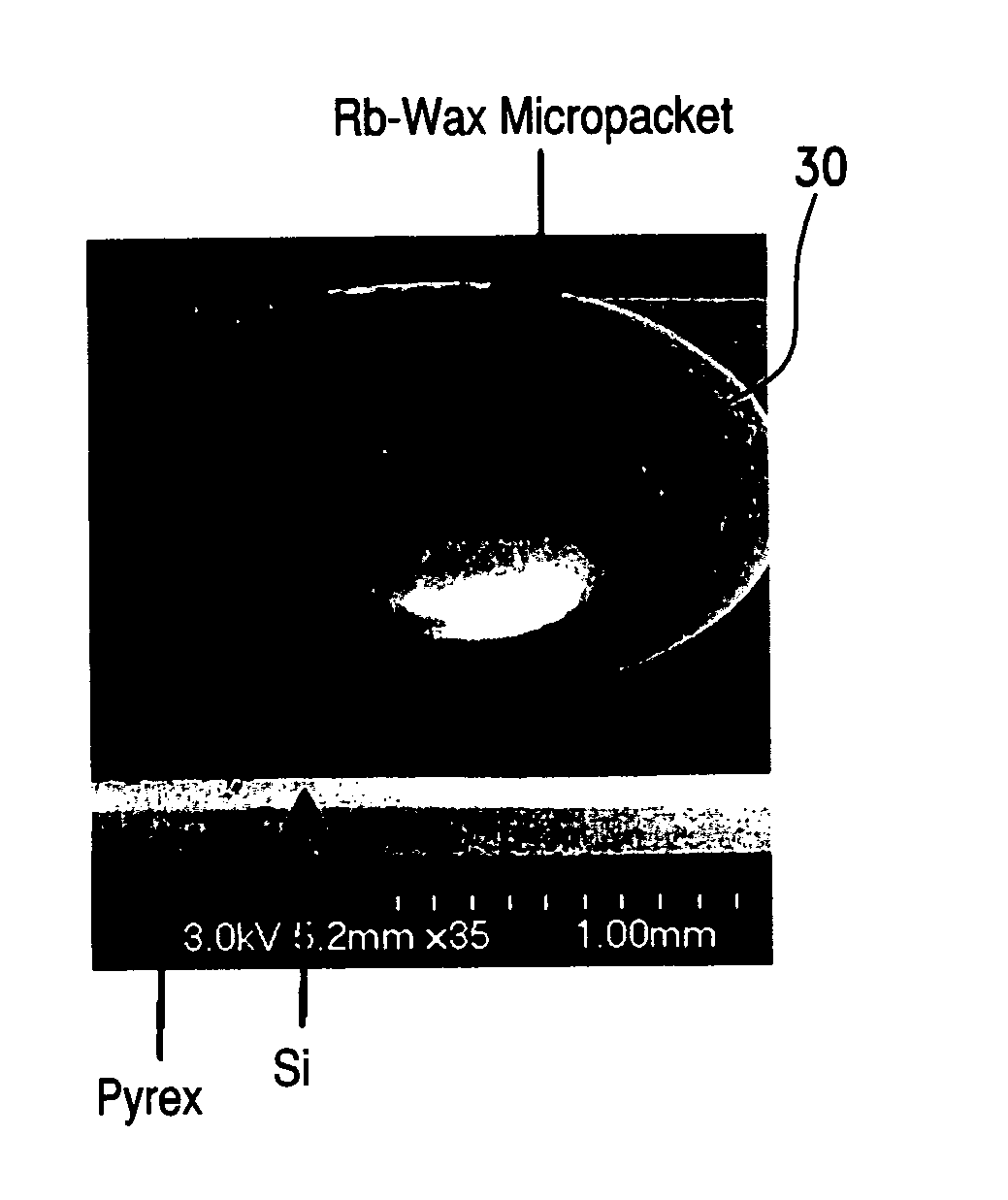
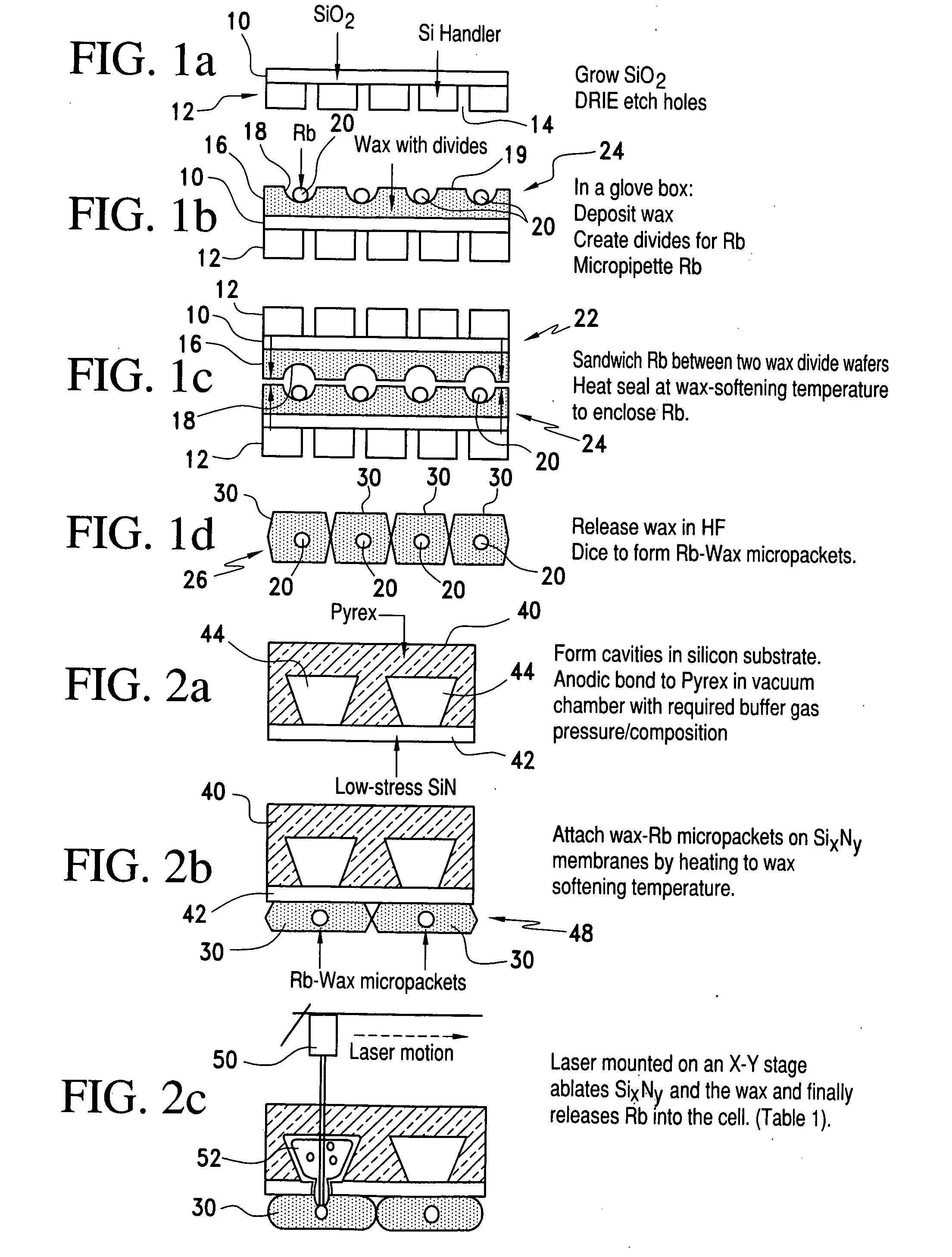
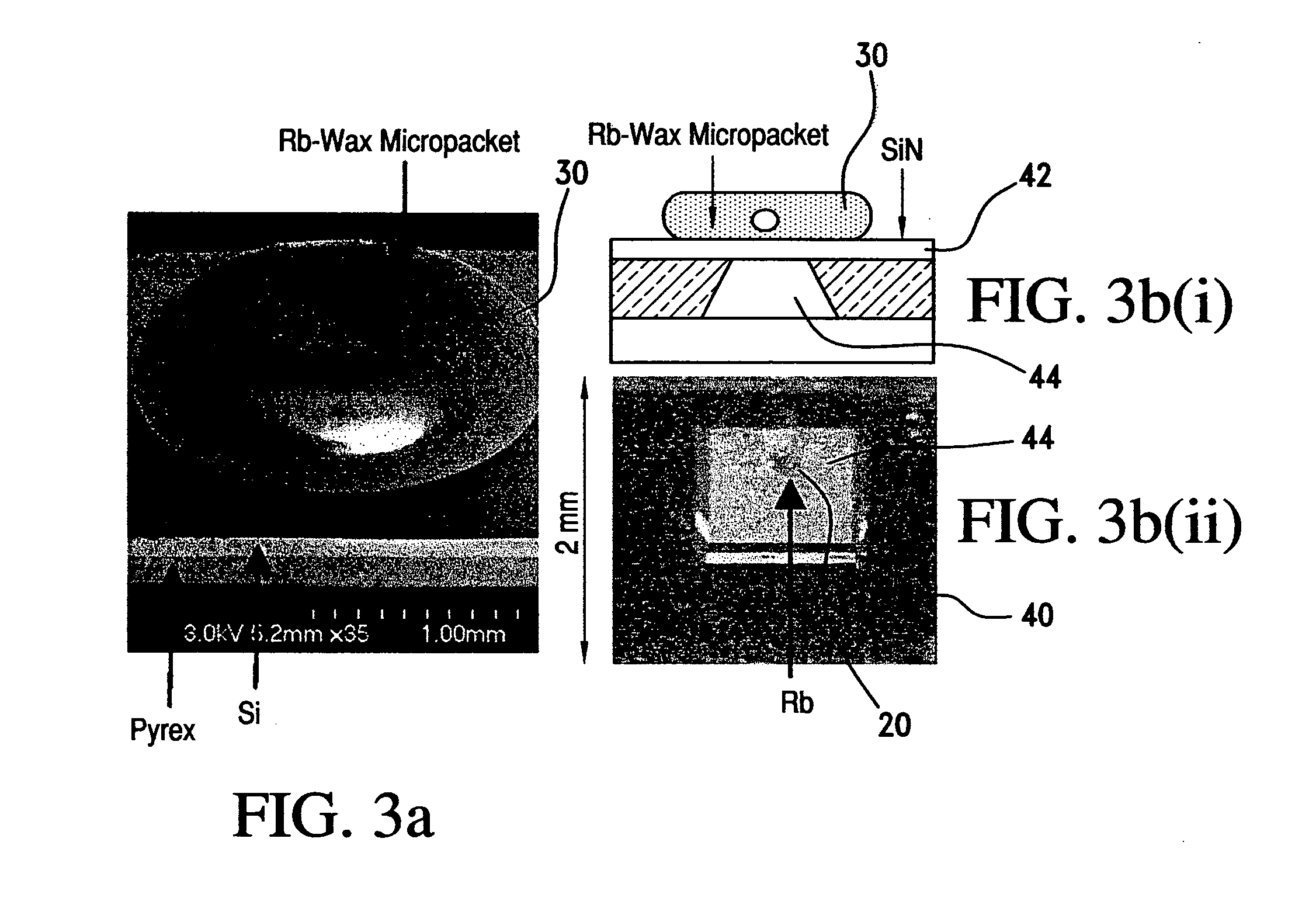
[0029] A Rb-wax micropacket array is thermally bonded to the silicon nitride (SixNy) membrane side of a wafer-scale cavity array and the enclosed Rb is released into the cavity by laser ablating the SixNymembrane through the glass wafer. The laser used for ablation is mounted on an X-Y stage to precisely ablate the wax in each micropacket to release the Rb in a controllable way into the cavity. Laser ablation thus offers a fast and effective way of delivering precise amount of Rb into the vapor cells.
[0030] Laser ablation may be done using a Coherent™ 355 nm laser system, and for large ablation times (>5 sec), the wax is ablated all the way through and results in the Rb reacting immediately with the atmosphere. For ablation times of ˜4 sec, the Rb is released and the wax forms a coating around the cavity. Although the effects of the wax wall coating remain unverified, one can conjecture that by carefully optimizing the ablation times and laser parameters, it is possible to form a thin uniform coating along the walls of the cavity that would result in increasing the coherence lifetimes of the alkali metals inside the vapor cells formed when using this process.

Problems solved by technology

The signals broadcast by GPS satellites are extremely low in power, making the GPS receivers highly susceptible to intentional jamming signals as well as to unintentional interference from sources transmitting in the same frequency band.
While the long-term precision of atomic clocks is unsurpassed, the size and power required to run them has prevented their use in a variety of areas, particularly in those applications requiring portability or battery operation.
In spite of these advantages, the power consumed by currently envisioned MEMS-based atomic clocks hasn't been reduced enough to permit their use in applications such as portable battery operated systems in long-term operations, including, for example, week-long missions for the military, months-long working of communication base units or even year / decade long operation for sensor node applications.
Solid state resonators (such as RF resonators based on quartz and silicon) are portable and energy efficient and so are often used in wrist watches and the like, but cannot provide an adequate reference signal because they have observable and random aging effects which cause their frequencies to shift in a non-predictable manner.
The use of highly reactive and low melting alkali metals and filling the vapor cells with the optimum pressure and composition of buffer gases thus impose a MEMS packaging challenge.
This can lead to residual impurities that cause long term drifts of the hyperfine resonance frequency.
However isolation of the cells from each other and dicing requires the use of a wax-sealing, which leads to low yield, and requires bulk rubidium delivery, which is inefficient and results in uncontrolled delivery of rubidium in each vapor cell.
However, the stringent requirements for the quality and apparatus needed for formation of wall coating is currently not compatible with MEMS processing.
Furthermore, alkylated silanes have been shown to degrade over long-term operations directly affecting the long-term stability of the atomic clock system.

Method used


Image

  • Alkali metal-wax micropackets for alkali metal handling
  • Alkali metal-wax micropackets for alkali metal handling
  • Alkali metal-wax micropackets for alkali metal handling

Examples


Embodiment Construction

[0047] Turning now to a more detailed description of the invention, the process for Alkali-Metal Wax Micropacket Fabrication, Figs 1a-1d schematically outline the sequence of process steps to form alkali metal wax micropackets.

[0048] Referring to FIG. 1a, a 1 μm thick layer of silicon dioxide (SiO2) 10 is deposited on a 4-inch silicon wafer 12 used as a handle substrate. Through-wafer holes 14 are etched through handle substrate 12 using deep reactive ion etching (DRIE) on the back side to serve as etch holes for the release process.

[0049] A thin uniform layer of wax 16 is deposited on top of the SiO2 layer 10 in the following way. The handling wafer 12 is placed on a hotplate with a level surface inside a nitrogen ambience glove box with low levels of oxygen and humidity within a few part per million. A measured amount of solid wax 16 is placed on the wafer 12, melted and spread using a microscope glass slide. The wafer is held above the melting point for a few minutes and rapidl...


PUM

PropertyMeasurementUnit
Temperatureaaaaaaaaaa
Volumeaaaaaaaaaa

Abstract

A method of making alkali-metal vapor cells by first forming microscale-wax micropackets with alkali metals inside allows fabrication of vapor cells at low cost and in a batch fabricated manner. Alkali metals are enclosed in a chemically inert wax to preform alkali metal-wax micropackets, keeping the alkali metals from reacting with the ambient surroundings during the vapor cell fabrication. This enables the deposition of precise amounts of pure alkali metal inside the vapor cells. Laser ablation of the alkali metal-wax micropackets provides a simple and effective way of releasing the enclosed metal. The method reduces the cost of making chip-scale atomic clocks and allows shipping of alkali vapor packets without contamination issues, thereby creating a technology for alkali-metal vendors to provide small packets of alkali metals.

Description

BACKGROUND OF THE INVENTION [0001] This application is a continuation of and claims priority to the filing date of U.S. provisional application Ser. No. 60 / 687,306, filed Jun. 6, 2005, the entire disclosure of which is hereby incorporated herein by reference. This application is also related to commonly owned U.S. provisional application Ser. No. 60 / 679,979, entitled RADIOACTIVE DECAY BASED STABLE TIME OR FREQUENCY REFERENCE SIGNAL SOURCE and filed May 12, 2005, the entire disclosure of which is also incorporated herein by reference. [0002] 1. Field of the Invention [0003] The present invention relates generally to a structure and method for fabrication of vapor cells adapted for use in making chip-scale atomic clocks (CSACs) via wafer-scale micro-machining processes. [0004] 2. Discussion of the Prior Art [0005] The need for more and more precise and stable time-keeping for a wide variety of applications has been on the rise, particularly in applications such as digital communicatio...

Claims


Application Information

Patent Timeline
IPC IPC(8): G01T1/18
CPCG04F5/14Y10T428/13Y10T428/162Y10T428/16
Inventor LAL, AMITRADHAKRISHNAN, SHANKAR
Owner CORNELL UNIVERSITY
Learn More