
Liquid crystal display panel with different substrate materials and method of making the liquid crystal display panel

a technology of liquid crystal display panel and substrate material, which is applied in the direction of manufacturing tools, instruments, optics, etc., can solve the problem of complicated cutting process

Inactive Publication Date: 2007-01-18
SAMSUNG DISPLAY CO LTD
View PDF5 Cites 13 Cited by
  • Summary
  • Abstract
  • Description
  • Claims
  • Application Information

AI Technical Summary

Benefits of technology

[0011] In another aspect, the invention is a method of making an LCD panel with different substrate materials. The method entails attaching a first substrate to a second substrate, wherein the first substrate includes a glass substrate and the second substrate includes a plastic substrate. The first and second substrates are irradiated with a laser beam to cut the first and the second substrates along a beam path.
[0012] In yet another aspect, the invention is a method of making an LCD panel. The method

Problems solved by technology

However, a problem with the LCD panel that includes both plastic substrate and glass substrate is that the cutting process is complicated.

Method used


Image

  • Liquid crystal display panel with different substrate materials and method of making the liquid crystal display panel
  • Liquid crystal display panel with different substrate materials and method of making the liquid crystal display panel
  • Liquid crystal display panel with different substrate materials and method of making the liquid crystal display panel

Examples


second embodiment

[0055]FIG. 5 shows a second embodiment where a sealant 300 is cut. The sealant 300 is directly cut by heat using a laser, similarly to the plastic substrate 210.

third embodiment

[0056]FIG. 6 shows a third embodiment where the second substrate 200 adhering to a dummy glass substrate 500 is cut. If necessary, the second substrate 200 is cut before being attached to a first substrate 100. After laser irradiation, the dummy glass substrate 500 is placed in contact with the cooling plate 600.

fourth embodiment

[0057]FIG. 7 shows a fourth embodiment where a second substrate 200 is cut without being attached to a dummy glass substrate 500. When the thickness d4 of the second substrate 200 is high, e.g. more than 0.7 mm, the dummy glass substrate 500 is not be used. Without the dummy glass substrate 500, it is not necessary to place the second substrate 200 in contact with the cooling plate 600 after laser irradiation. Therefore, laser is shined onto the second substrate from the top, allowing the first substrate 100 to easily contact the cooling plate 600.


PUM

PropertyMeasurementUnit
Temperatureaaaaaaaaaa
Coloraaaaaaaaaa
Areaaaaaaaaaaa

Abstract

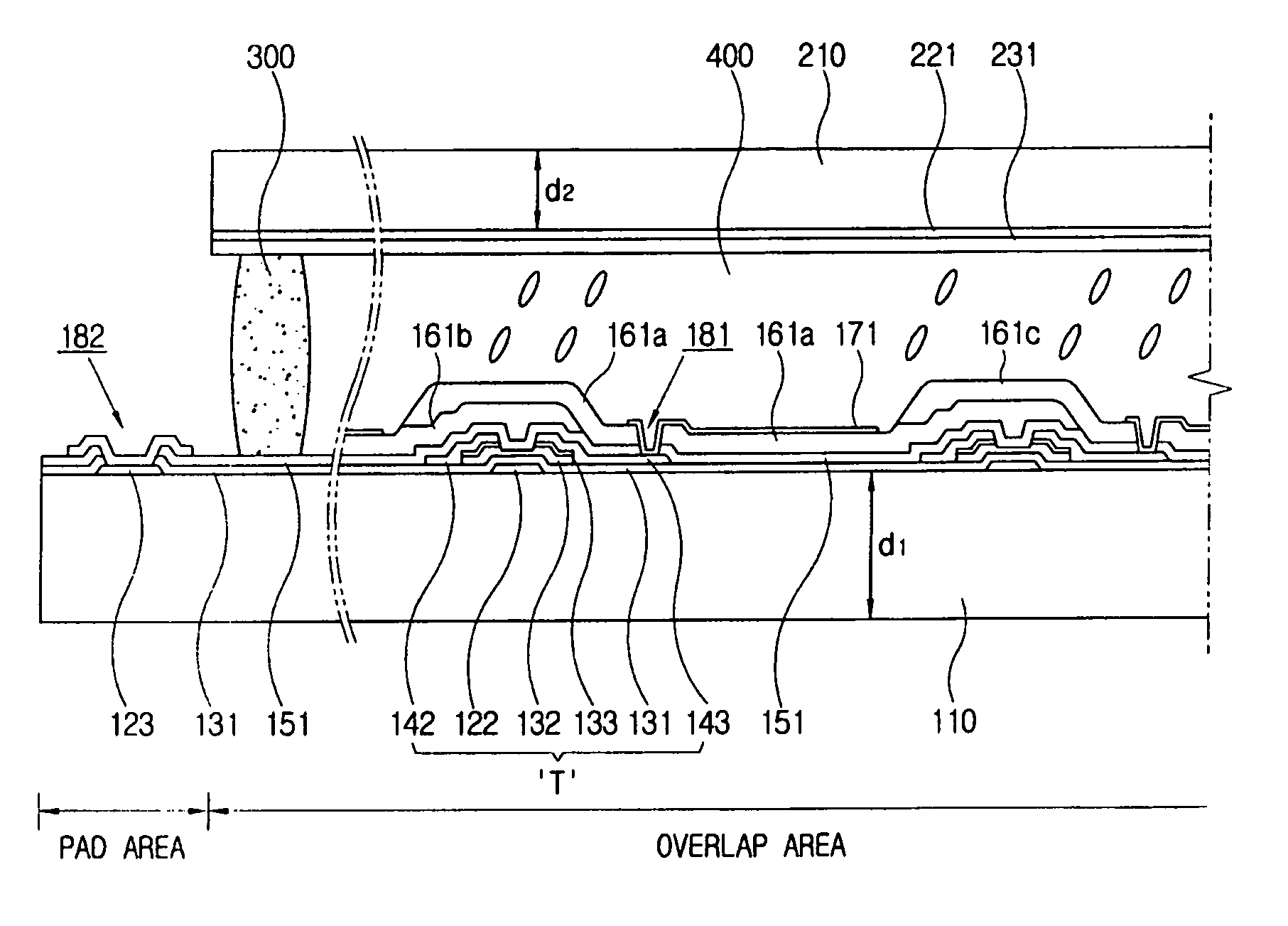
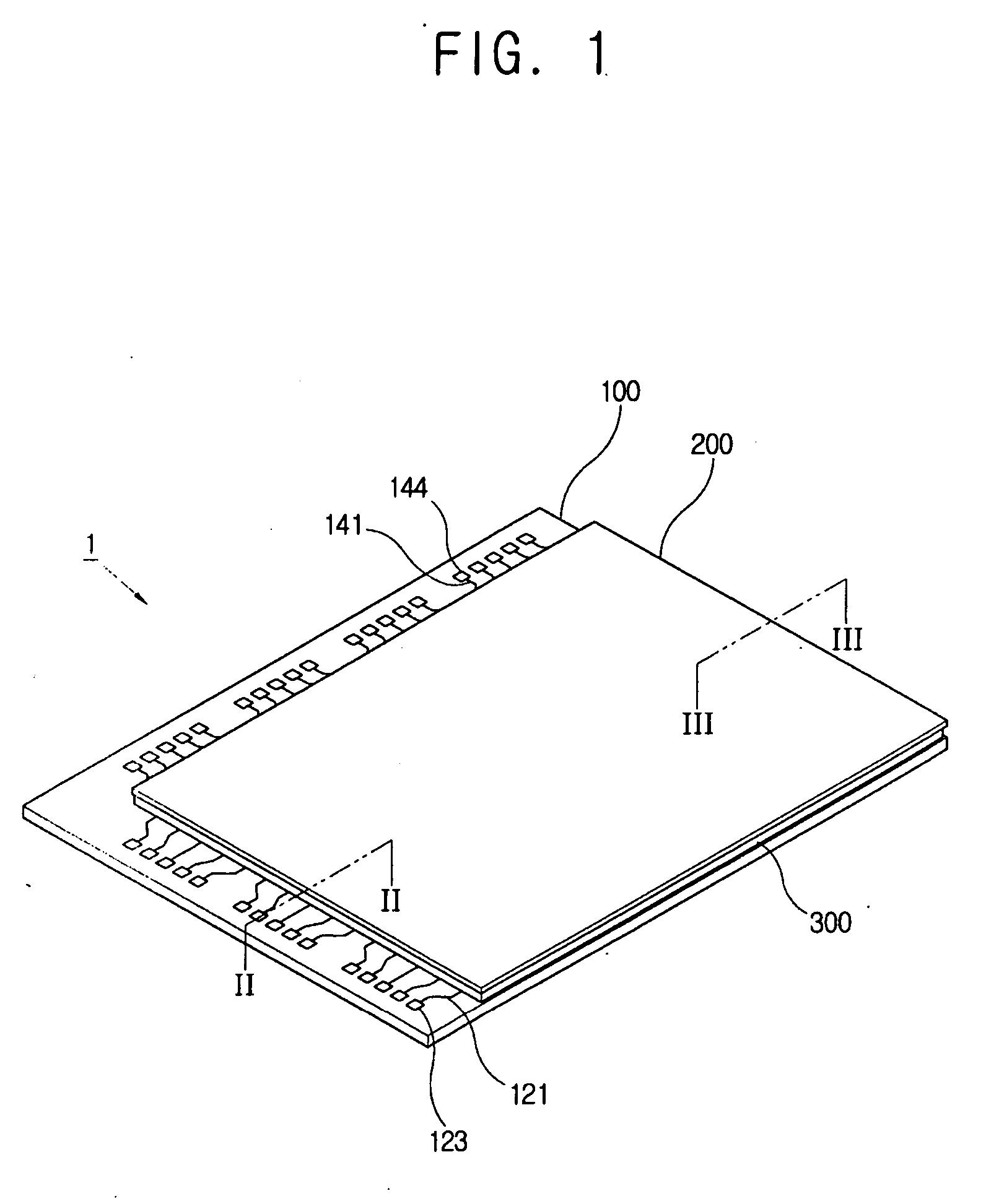
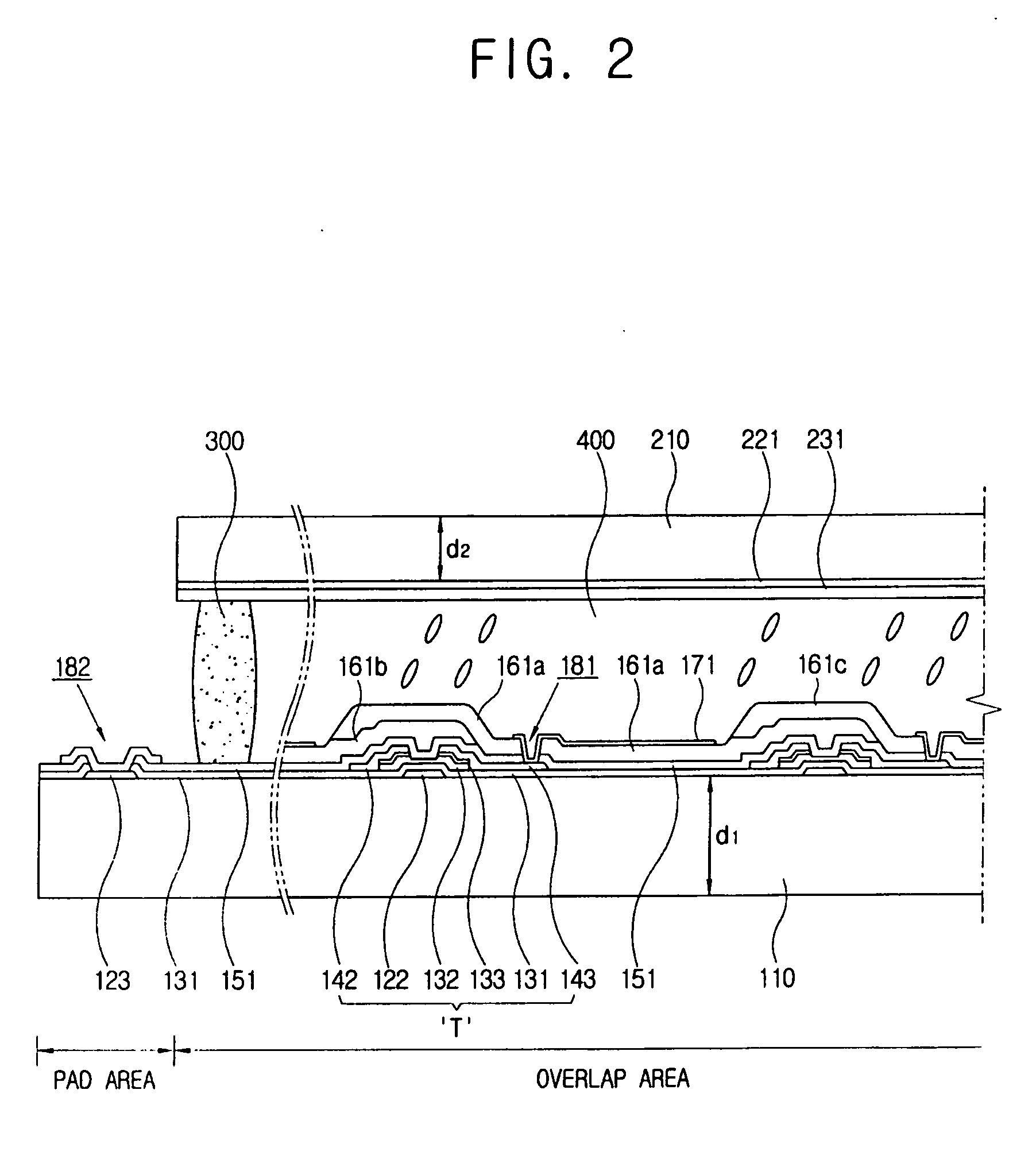
An LCD panel with mixed substrate materials and a method of making the LCD panel are presented. The LCD panel is made of a first substrate, a second substrate disposed substantially parallel to the first substrate, and a liquid crystal layer disposed between the first substrate and the second substrate. The first substrate includes a glass substrate, a TFT formed on the glass substrate, and a color filter formed on the TFT. The second substrate includes a plastic substrate and a common electrode formed on the plastic substrate. Forming the color filter on the TFT eliminates the need to form black matrices on the second substrate, preventing misalignment of the two substrates due to different heat sensitivities. Since there is no concern of substrate misalignment caused by heat, laser beam can be used to cut the substrates during the manufacture of the LCD panel.

Description

CROSS-REFERENCE TO RELATED APPLICATIONS [0001] This application claims the benefit of Korean Patent Application No. 2005-0048794, filed on Jun. 8, 2005 in the Korean Intellectual Property Office, which is hereby incorporated by reference for all purposes. BACKGROUND OF THE INVENTION [0002] 1. Field of the Invention [0003] The present invention relates to a liquid crystal display panel, and more particularly to a method of cutting the substrates of a liquid crystal display panel. [0004] 2. Description of the Related Art [0005] Typically, a liquid crystal display (“LCD”) device includes an LCD panel having a first substrate, a second substrate disposed opposite to the first substrate, and a liquid crystal layer disposed between the two substrates. Thin film transistors (“TFTs”) are formed on the first substrate. Since the LCD panel does not emit light, the LCD is often used in conjunction with a backlight unit disposed behind the first substrate to act as a light source. [0006] Light ...

Claims


Application Information

Patent Timeline
IPC IPC(8): H01L29/04H01L29/15H01L31/036B23K26/00B23K26/38B28D5/00G02F1/13G02F1/1333G02F1/1335G02F1/1368
CPCG02F1/133305G02F2001/136222G02F1/1362G02F1/1341G02F1/136222G02F1/1345G02F1/13
Inventor HONG, WANG-SULEE, WOO-JAE
Owner SAMSUNG DISPLAY CO LTD
Learn More