Phosphor tape article
a technology of phosphor tape and tape articles, which is applied in the direction of basic electric elements, electrical equipment, and semiconductor devices, can solve the problems of inability to accurately control the amount of phosphor deposited, the difficulty of dispense of high phosphor loading, and the decrease in size (volume). achieve the effect of greater color consistency and/or predictability
- Summary
- Abstract
- Description
- Claims
- Application Information
AI Technical Summary
Benefits of technology
Problems solved by technology
Method used
Image
Examples
example 1
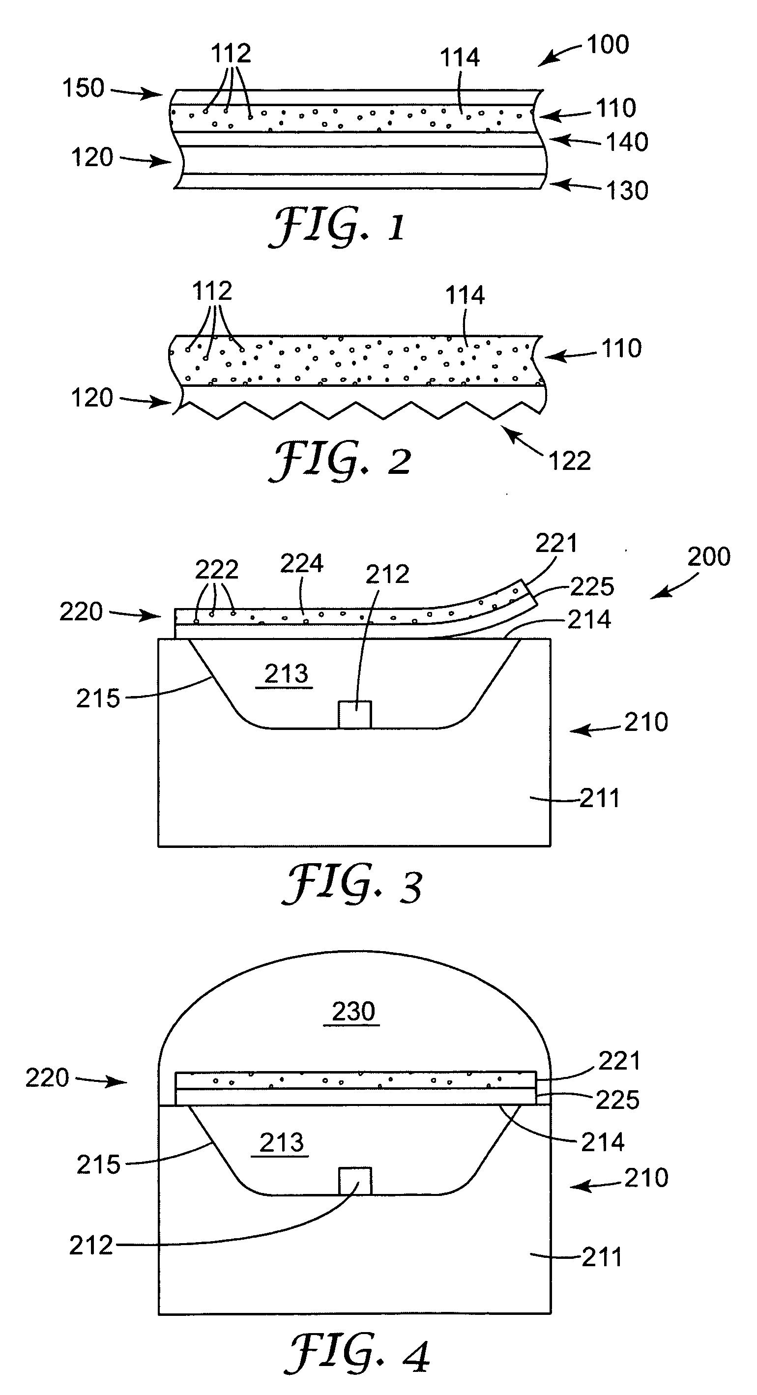
[0050] A sample of phosphor tape was made by applying a pressure sensitive adhesive to a phosphor-loaded film layer. The phosphor-loaded film layer contained cerium-doped yttrium aluminate (YAG:Ce) phosphor in a UV-curable binder. The phosphor-loaded film was made from a paste prepared by hand mixing 13.63 grams of YAG:Ce phosphor (designated QMK58 / F-U1 by Phosphor Technology, Ltd. of Stevenage, England) into 20.45 grams of UV-curable resin (designated NOA 81 by Norland Products, Cranbury, N.J.). The paste was coated onto a sheet of polyethylene terphthalate (PET) by hand using the 100 micrometer gap of a square multiple clearance applicator (designated PAR-05353 by BYK-Gardner USA, Columbia, Md. The wet film was cured by placing it below a bank of UV bulbs (designated F15T8 / 350BL by Osram Sylvania, Danvers, Mass.) for about 5 minutes. A pressure-sensitive adhesive (designated Optically Clear Adhesive (OCA) specifically a cross-linked iso-octyl acrylate / acetic acid (90 / 10)PSA) was c...
example 2
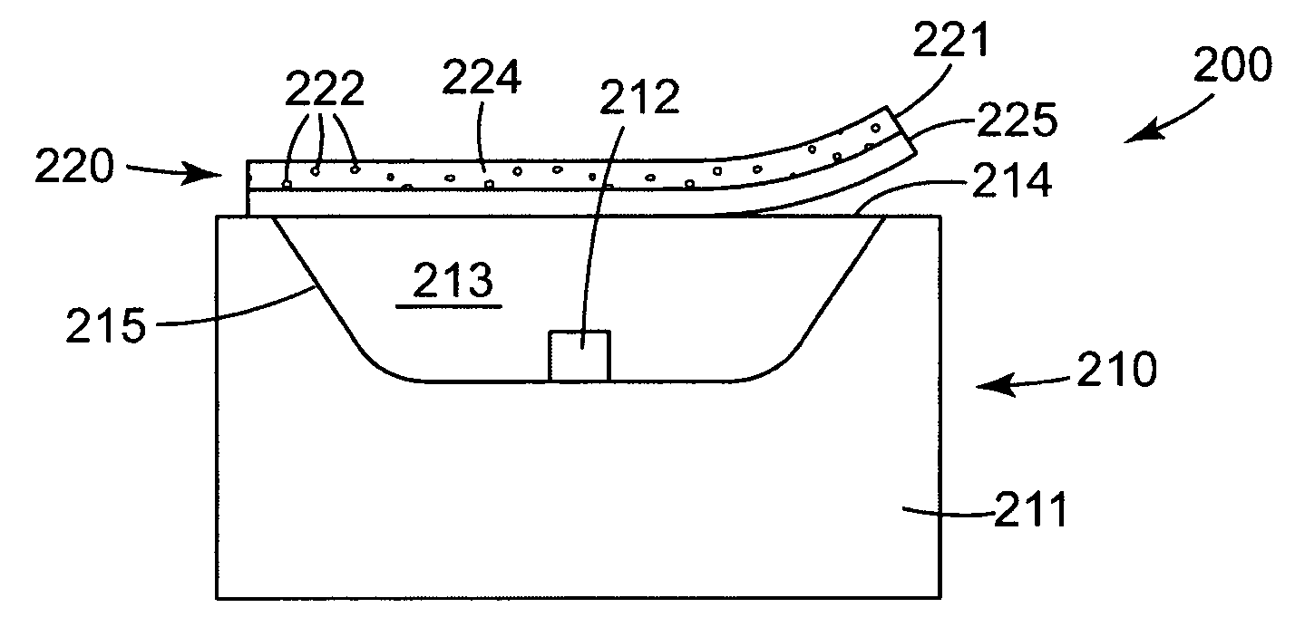
[0051] The phosphor tape prepared in Example 1 was adhered to an encapsulated blue LED (commercially available from Stanley Electric Company, Tokyo, Japan) to produce a white LED. To attach the film, the release liner was removed and the LED top surface was placed against the exposed adhesive. The film was firmly pressed against the encapsulant to ensure that the adhesive touched the encapsulant and had a good optical contact. The film was cut to the size of the LED. The PET substrate was then peeled away from the phosphor-loaded layer, leaving just the phosphor-loaded layer bonded to the LED package by the pressure sensitive adhesive.
[0052] The optical output of the assembled white LED was measured using a spectroradiometer (designated OL 770-LED by Optronic Laboratories, Inc., Orlando, Fla.) fitted with an integrating sphere (designated OL IS-670-LED by Optronic Laboratories, Inc., Orlando, Fla.). The spectroradiometer was calibrated to report the radiant energy entering the inte...
PUM
 Abstract
Description
Claims
Application Information
 - R&D
- Intellectual Property
- Life Sciences
- Materials
- Tech Scout
- Unparalleled Data Quality
- Higher Quality Content
- 60% Fewer Hallucinations
Browse by: Latest US Patents, China's latest patents, Technical Efficacy Thesaurus, Application Domain, Technology Topic, Popular Technical Reports.
© 2025 PatSnap. All rights reserved.Legal|Privacy policy|Modern Slavery Act Transparency Statement|Sitemap|About US| Contact US: help@patsnap.com


