Light emitting diode with larger illumination area

a technology of light-emitting diodes and illumination areas, which is applied in the direction of basic electric elements, electrical equipment, and semiconductor devices, can solve the problems of increasing the cost of illumination devices and consuming a lot of energy of conventional tungsten lamps with higher power, and achieves the effects of improving shadow, increasing illumination area, and increasing illumination area

Inactive Publication Date: 2006-12-21
NANOFORCE TECH CORP
View PDF3 Cites 7 Cited by
  • Summary
  • Abstract
  • Description
  • Claims
  • Application Information

AI Technical Summary

Benefits of technology

[0008] A light emitting diode with larger illumination area in accordance with the present invention includes a shielding layer disposed over an incident plane on a LED chip and length of the shielding layer may be longer, shorter or equal to that of the incident plane of the LED chip. Thereby, light emitted from the LED chip passes through the shielding layer and has diffraction so as to make LED with different packages have larger illumination area. Furthermore, the shielding layer includes at least an aperture etched thereof, or metal particles mixed with transparent particles, printed on the LED chip so as to make light from the LED chip passes through a single-slit, double-slit or multiple slit formed by the aperture or transparent particles on the shielding layer to generate new wavefronts and improves shadow on near-field of the original diffraction. Thus an increased illumination area is formed on near field. Therefore, the LED according to the present invention becomes a bottom lighting type back light source.

Problems solved by technology

However, conventional tungsten lamps with higher power consume quite a lot of energy.
Thus the cost of illumination devices is increased.

Method used


Image

  • Light emitting diode with larger illumination area
  • Light emitting diode with larger illumination area
  • Light emitting diode with larger illumination area

Examples


Embodiment Construction

[0033] The present invention provides a LED with larger illumination area to overcome above disadvantages.

[0034] The following SMD(surface mounting device) LED, lamp LED and PCB(printed circuit board) LED are taking as examples to explain the present invention. The present invention is applied to LED with different packages so as to make illumination area of point source LED change into illumination area of surface light source.

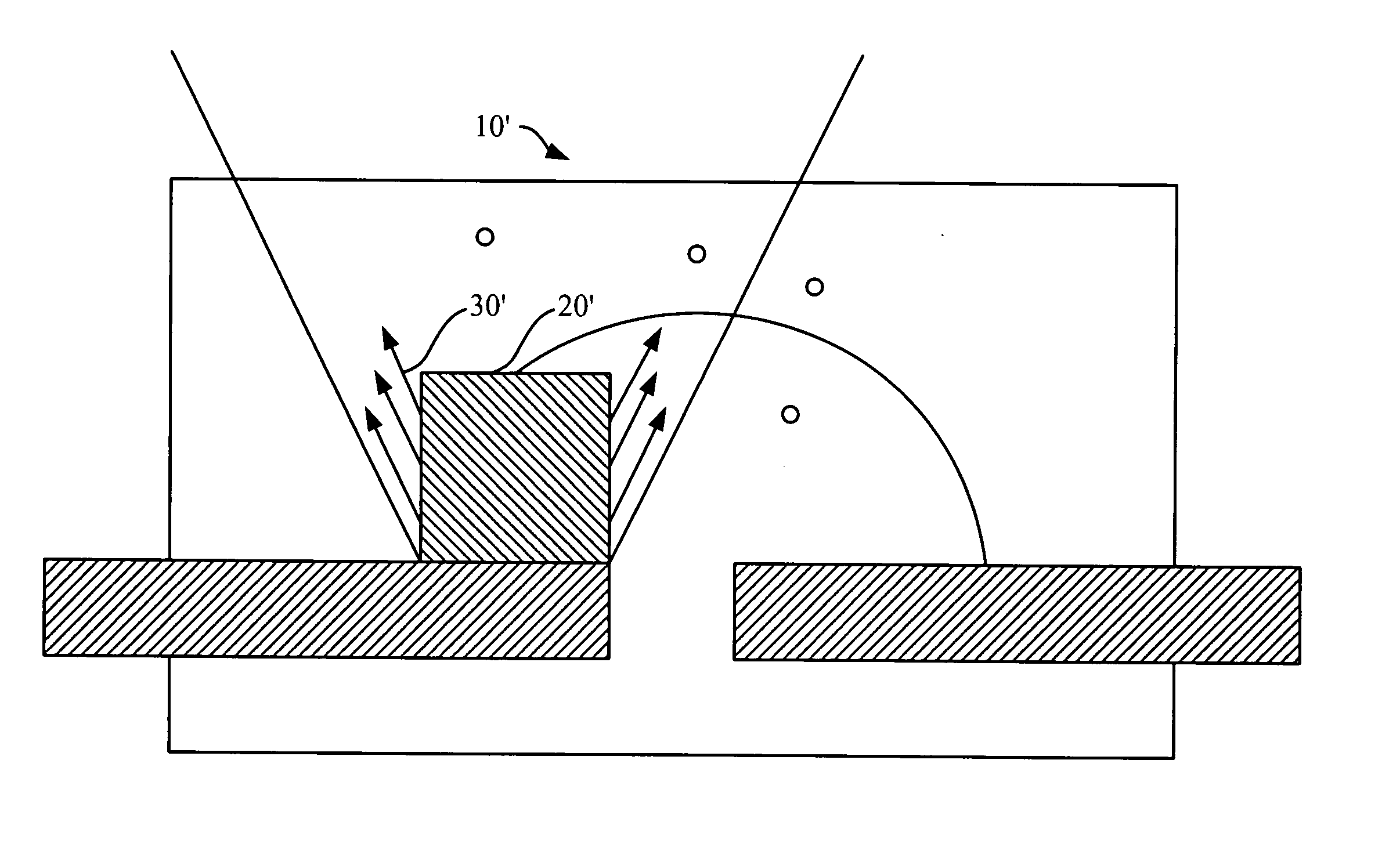
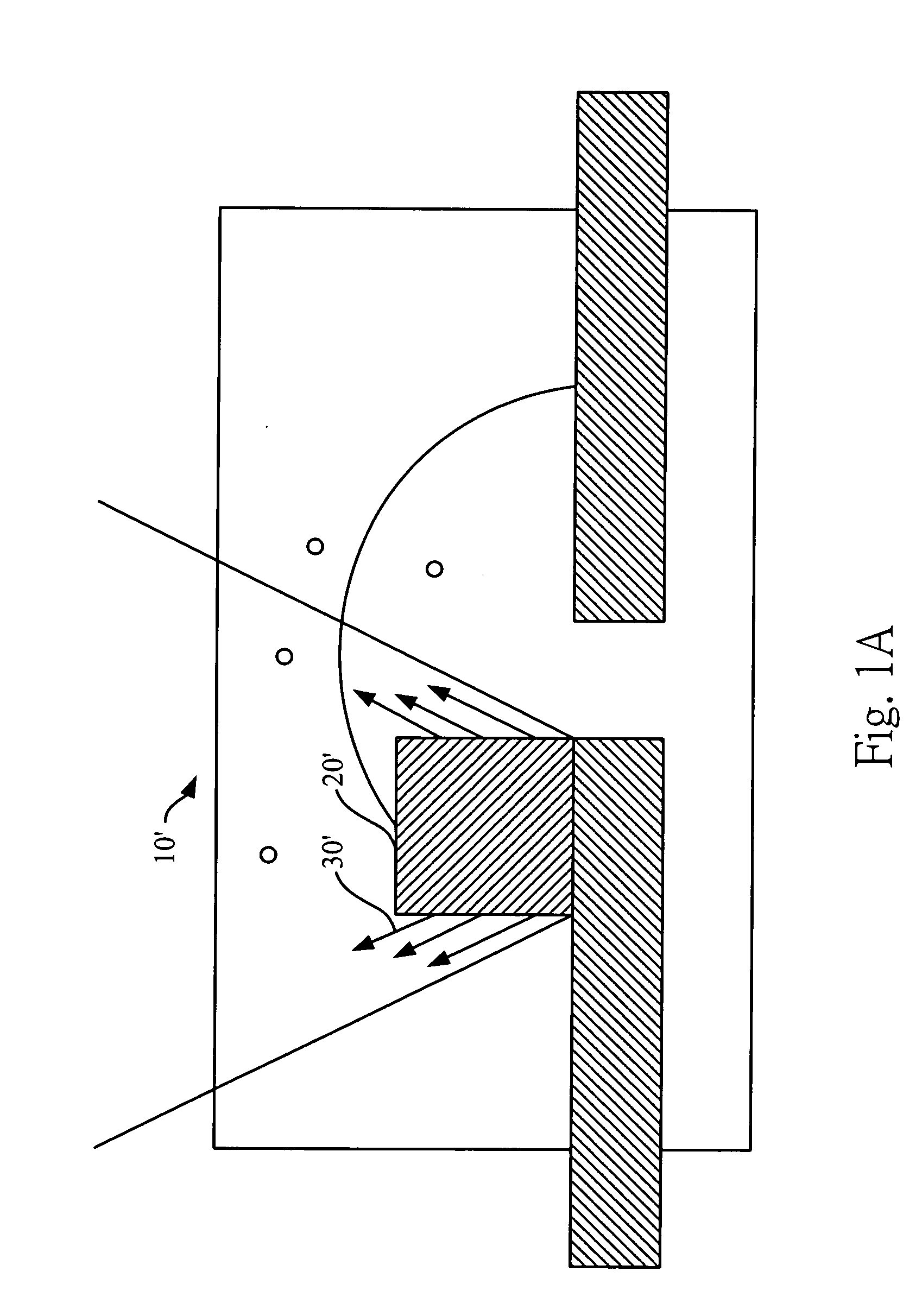
[0035] Refer to FIG. 2, a LED in accordance with the present invention consists of a LED chip 10 and a shielding layer 20 that is disposed over an incident plane 12 on the LED chip 10. The length of the shielding layer 20 is longer than that of the incident plane 12 on the LED chip 10. When light emitted from the LED chip 10 arrives the shielding layer 20, a first wavefront 30 caused by diffraction is generated. After various portions of the first wavefront 30 in spherical shape propagating a certain distance, the light waves interacts with one another to f...


PUM


Abstract

The present invention relates to a light emitting diode with larger illumination area that includes a LED chip and a shielding layer. The shielding layer is disposed over an incident plane of the LED chip and its length is longer, equal to or shorter than the length of the incident plane of the LED chip. Thus diffraction generates by light emitted from the LED chip passing through the shielding layer so as to increase illumination area of the LED with more uniform brightness.

Description

BACKGROUND OF THE INVENTION [0001] The present invention relates to a light emitting diode, especially to a light emitting diode that increases illumination area of light source. [0002] Since there is an illumination device, the most common light source is a point source such as tungsten lamps. However, conventional tungsten lamps with higher power consume quite a lot of energy. Thus people in industry or research institute in various countries are dedicated to developing new light source for improving shortcomings of conventional tungsten lamps. Therefore, high-luminous LED chip and the related lamp design is invented to meet such kind of requirements. LED becomes new type point source. [0003] Light emitting diode (LED) is a fine solid-state light source made of semiconductor material. The device that turns electricity into light features on the compact structure, with long lifetime, low driving voltage, fast reaction, and good shock resistance. It can also be applied in various ap...

Claims


Application Information

Patent Timeline
Patent Type & Authority Applications(United States)
IPC IPC(8): H01L33/00H01L33/44H01L33/58
CPCH01L33/44H01L33/58H01L2924/3025H01L2924/00H01L2224/48091H01L2224/48247H01L2224/48257H01L2924/181
Inventor HUANG, FU-KUO
Owner NANOFORCE TECH CORP
Why Eureka
Try Eureka