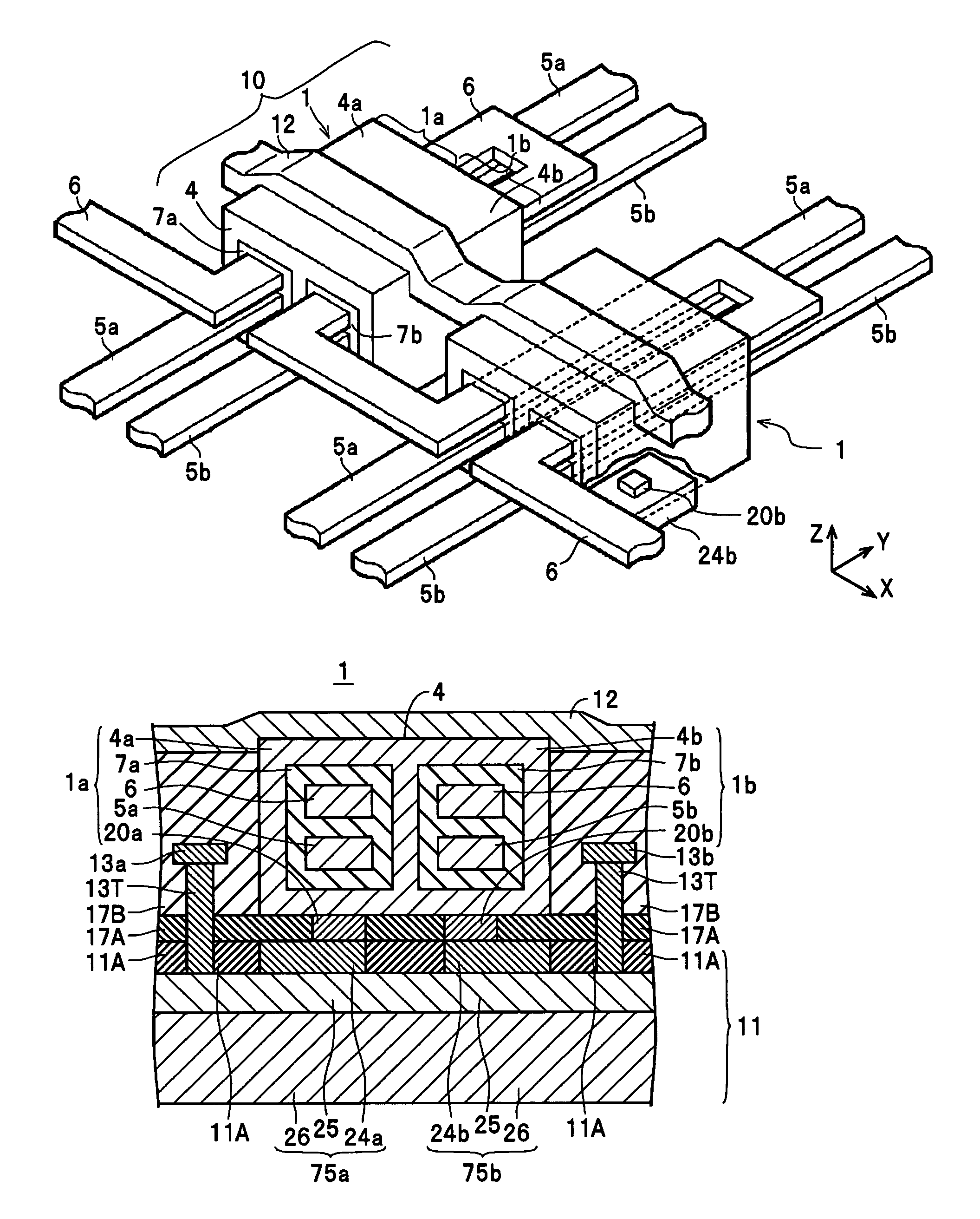
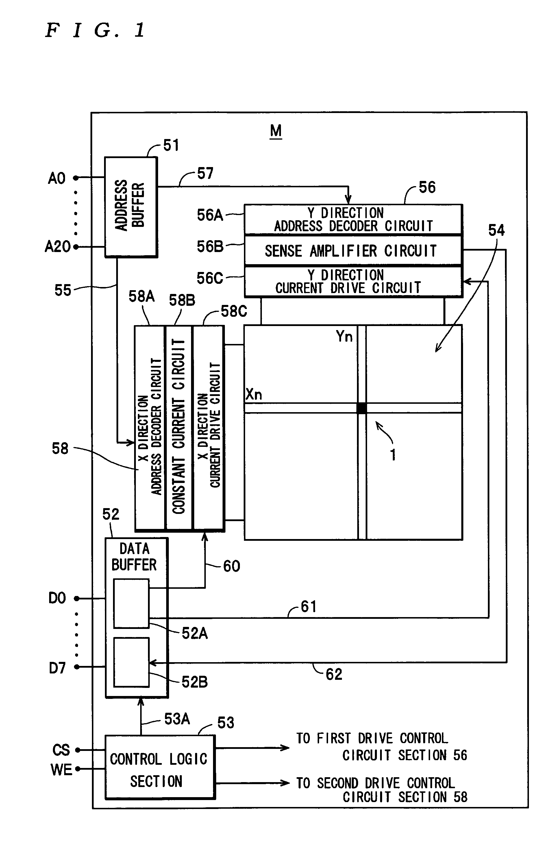
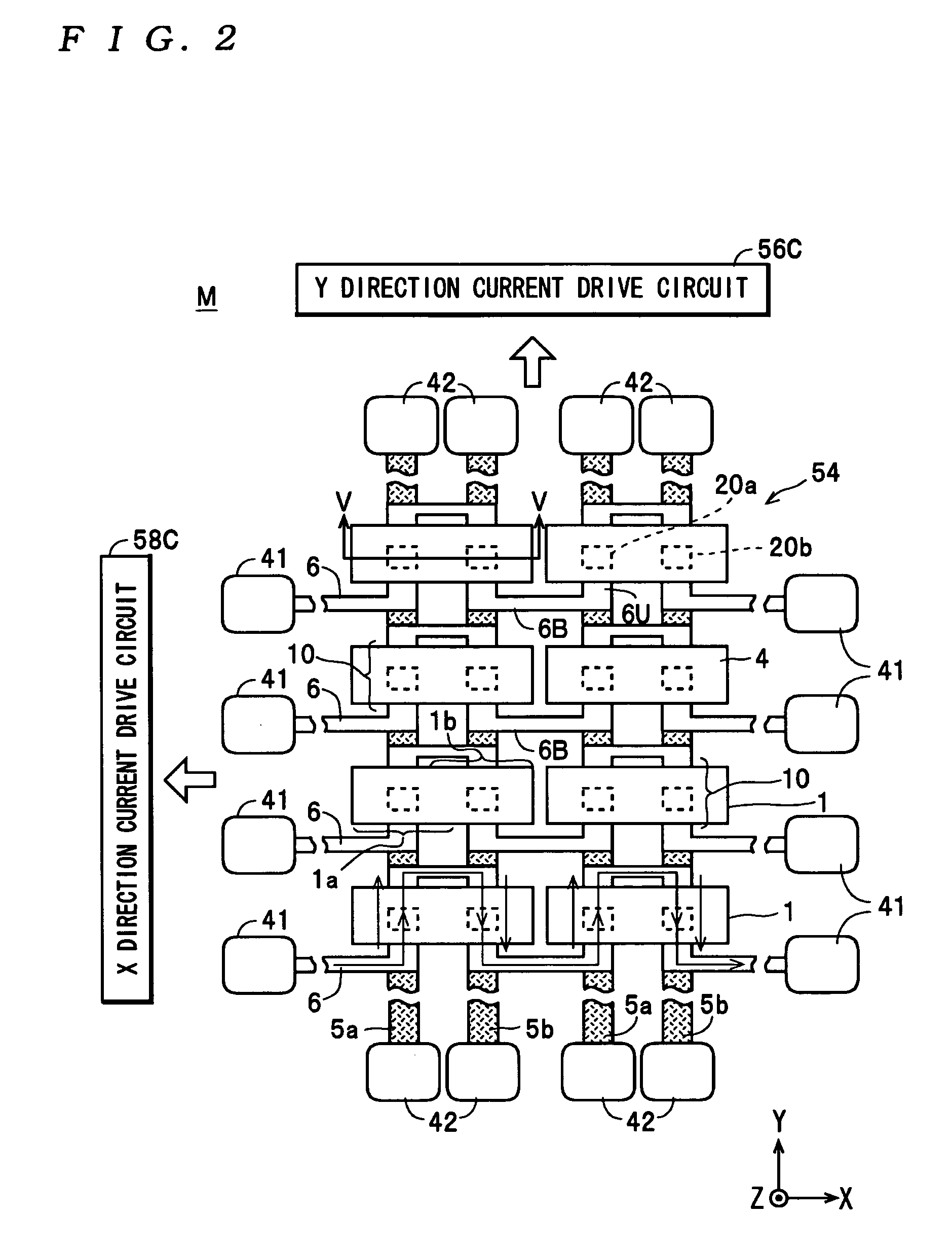
[0025] The magnetic
memory cell and the magnetic memory device according to the present invention comprises an annular
magnetic layer through which extends at least one conductor that generates a
magnetic field, and a laminate configured so as to include: a first magneto-sensitive layer, a magnetization direction of which is changed by the magnetic field in the annular magnetic layer; and a magnetoresistive effect revealing body disposed on a surface of the first magneto-sensitive layer so that an
electric current flows in a direction perpendicular to a laminating surface of the laminate, and the thickness of the first magneto-sensitive layer is set within a range of not less than 0.5 nm to not more than 40 nm. Therefore, it is possible to ensure a thickness of 0.5 nm or more, which enables the first magneto-sensitive layer to be stably manufactured as a magnetic film. This makes it possible to largely enhance the yield of the magnetic memory device. Further, since the thickness of the first magneto-sensitive layer is set at not more than 40 nm, a
demagnetizing field due to the thickness is decreased, thereby making it possible to reduce the current value of a
write current required for inverting the magnetization direction of the first magneto-sensitive layer, while ensuring the balance between the write currents flowing through the storage element to some degree, to thereby efficiently change the magnetization direction of the first magneto-sensitive layer.
[0026] The magnetic
memory cell and the magnetic memory device according to the present invention comprise a plurality of storage elements each having an annular magnetic layer through which extends at least one conductor that generates a magnetic field, and a laminate configured so as to include: a first magneto-sensitive layer, a magnetization direction of which is changed by the magnetic field in the annular magnetic layer; and a magnetoresistive effect revealing body disposed on a surface of the first magneto-sensitive layer so that an electric current flows in a direction perpendicular to a laminating surface of the laminate, wherein the plurality of annular magnetic
layers are configured so as to be arranged side by side such that directions of respective axes coincide with each other, and so as to share a predetermined portion of each with each other, and the thickness of the first magneto-sensitive
layers is defined within a range of not less than 0.5 nm to not more than 40 nm. Therefore, it is possible to ensure a thickness of 0.5 nm or more, which enables the first magneto-sensitive layers to be stably manufactured as
magnetic films. This makes it possible to largely enhance the yield of the magnetic memory device. Further, since the thickness of the first magneto-sensitive layers is set at not more than 40 nm, a
demagnetizing field due to the thickness is decreased, thereby making it possible to reduce the current values of write currents flowing through the storage elements, while ensuring the balance between the write currents required for inverting the magnetization direction of the first magneto-sensitive layer to some degree, to thereby efficiently change the magnetization directions of the first magneto-sensitive layers.
[0027] Further, according to the
memory cell and the magnetic memory device according to the present invention, the plurality of magneto-sensitive layers are configured so as to be magnetized in directions antiparallel to each other by magnetic fields. This makes it possible to always align the directions of the magnetic fields generated in the shared portion of the annular magnetic layers when electric currents are caused to flow through the conductors of the pair of storage elements, and therefore it is possible to reliably increase the
magnetic flux density in the shared portion of the annular magnetic layers. This makes it possible to increase the strengths of the circulating magnetic fields within the annular magnetic layers, thereby making it possible to invert the magnetization directions of the first magneto-sensitive layers with smaller write currents.
[0028] Further, according to the memory cell and the magnetic memory device according to the present invention, since the thickness of the first magneto-sensitive layers is set at not more than 30 nm, the
demagnetizing field due to the thickness is further decreased, thereby making it possible to further reduce the current values of write currents required for inverting the magnetization directions of the first magneto-sensitive layers, while further balancing the write currents flowing through the storage elements, to thereby efficiently change the magnetization directions of the magneto-sensitive layers.
[0029] Further, according to the memory cell and the magnetic memory device according to the present invention, a plurality of the conductors are configured to extend in parallel with each other in a region where the conductors extend through the annular magnetic layers. Therefore, compared with a construction in which a plurality of conductors cross each other, synthetic magnetic fields produced by passing electric currents through the conductors can be increased, and therefore it is possible to more efficiently invert the magnetization directions of the first magneto-sensitive layers.
[0030] Further, according to the memory cell and the magnetic memory device according to the present invention, the laminate comprises a second magneto-sensitive layer which can be magnetically exchange-coupled with the first magneto-sensitive layer. This makes it possible to select a material having a high
polarizability as a material for forming the second magneto-sensitive layer, and hence it is possible to increase the rate of change in the
magnetoresistance of the storage element.


