
Method for producing alloy deposits and controlling the nanostructure thereof using negative current pulsing electro-deposition, and articles incorporating such deposits

a technology of negative current pulsing and electro-deposition, which is applied in the direction of electrolysis components, electrolysis processes, transportation and packaging, etc., can solve the problems of limited shape, difficult processing of nanocrystalline metals, and limited compaction methods

Active Publication Date: 2006-12-07
MASSACHUSETTS INST OF TECH
View PDF15 Cites 82 Cited by
  • Summary
  • Abstract
  • Description
  • Claims
  • Application Information

AI Technical Summary

Problems solved by technology

Processing nanocrystalline metals is regarded as challenging, because they necessarily exhibit far-from-equilibrium microstructures.
The compaction method inevitably incorporates impurities into the material, which is undesirable.
The compaction method is also limited to shapes that can be formed from compacted sintered powder, which shapes are limited.
Relatively large amounts of energy are needed to practice the severe plastic deformation methods.
Further, they are not easily scalable to industrial scales, and cannot generally produce the finest grain sizes in the nanocrystalline range without a significant increase in costs.
An electrodeposition process is scalable and requires relatively low energy.
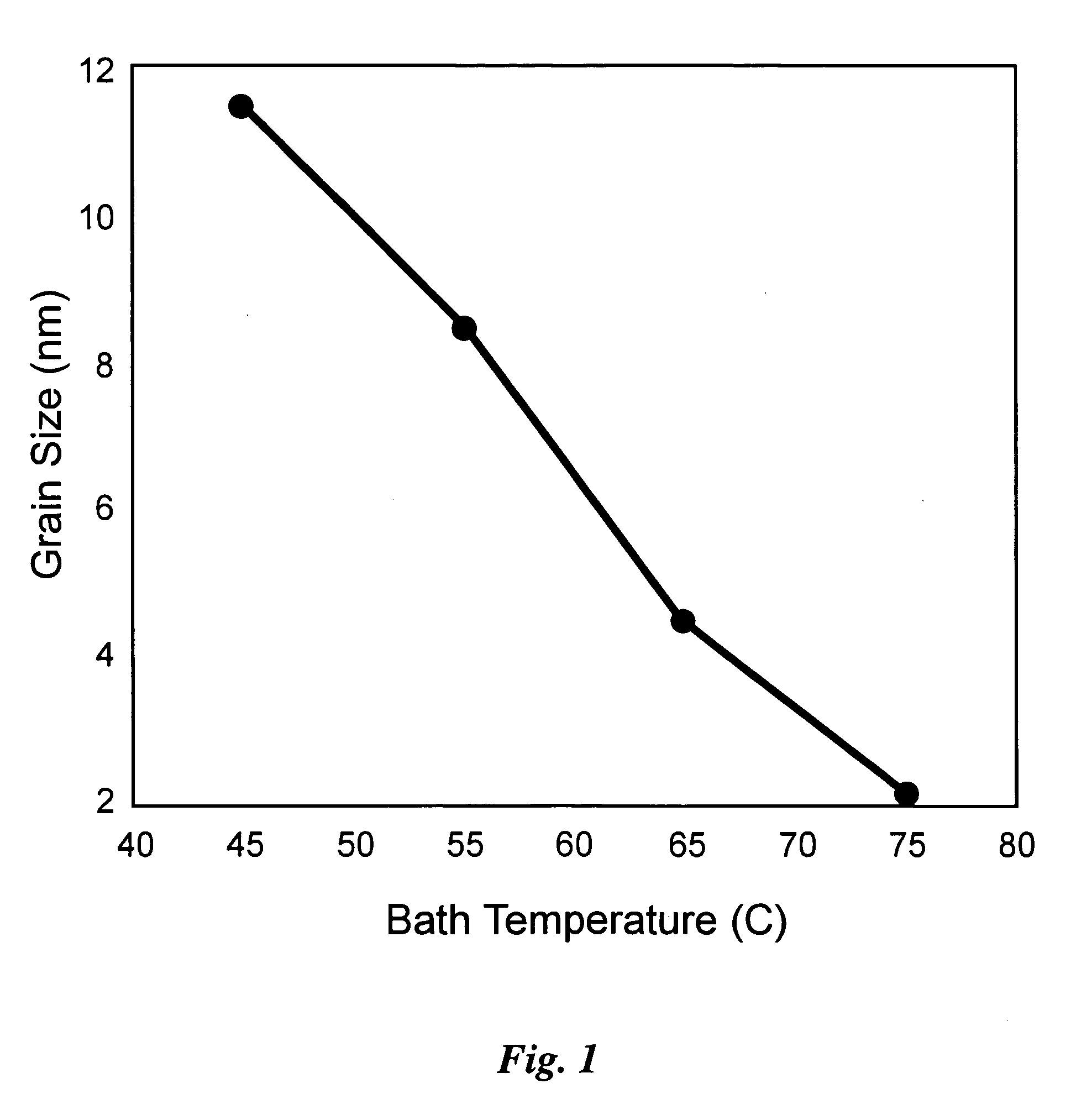
While it is true that grain size can be specified by controlling liquid temperature, other characteristics of the deposit produced with temperature control are undesirable.
In addition to this poor homogeneity, bath temperature control suffers from additional undesirable problems.
Changing bath temperature during a deposit is time consuming and highly energy consuming in large systems.
Thus, it is not possible to change grain size and composition without significant difficulty, either during a single deposition run or from one run to the next run.
Thus, it is difficult to achieve a microstructure that is graded or layered with respect to grain size within a single deposit.
Thus, a control method that requires changing the liquid temperature has undesirable complexity and costs associated therewith.
However, doing so also prohibits producing sequential, differently composed deposits without chemical alterations to the liquid, again, an added complexity.
Changing the liquid composition, and / or its temperature necessarily results in system idle times. These idle times add cost to the process.
Thus, a difficulty with electrodepositing nanocrystalline deposits using either DC plating or UPP, is that it is not possible to obtain deposits having grain size within limits as precisely as may be desired.
Changing the temperature or the composition of the bath is cumbersome.
Moreover, it is not possible to produce a deposit having a nano-structure that varies through its thickness, especially if cracks and voids are to be avoided.
Similarly, it is not possible to obtain deposits having composition as precisely as may be desired.
While this method can be used to control grain size (and also composition) it is inherently limited by the range of current densities that can be used while still achieving a homogeneous, crack and void free deposit of sufficient thickness.
A high current density will result in highly stressed, cracked and voided deposits while a low current density will result in a slow deposition rate.
Thus the range of grain sizes that can be achieved by this method are limited to a degree that makes it operationally unpractical.

Method used


Image

  • Method for producing alloy deposits and controlling the nanostructure thereof using negative current pulsing electro-deposition, and articles incorporating such deposits
  • Method for producing alloy deposits and controlling the nanostructure thereof using negative current pulsing electro-deposition, and articles incorporating such deposits
  • Method for producing alloy deposits and controlling the nanostructure thereof using negative current pulsing electro-deposition, and articles incorporating such deposits

Examples


example

[0055] Using BPP to control crystal grain size in the nano-meter range has been reduced to practice, for instance for the particular case of a binary alloy of nickel-tungsten. This alloy was deposited with the liquid bath composition and plating parameters as given in Table 1, using an inert platinum electrode 342, nominally designated an anode and a copper electrode 340, nominally designated a cathode, in a 2 liter bath, as shown schematically with reference to FIG. 3. A pulsed current was used, having a negative current portion, the amplitude of which was varied for different specimen runs from 0 to negative 0.3 A / cm2 at a constant pulse time of 3 ms. The positive portion of the pulse always had an amplitude of +0.2 A / cm2, and a duration of 20 ms.

TABLE 1Deposition conditions for nickel-tungstenNickel sulfate hexahydrate (NiSO4.6H2O)0.06 MSodium tungstate hexahydrate (Na2WO4.2H2O)0.14 MSodium citrate dihydrate (Na3C6H5O7.2H2O) 0.5 MAmmonium chloride (NH4Cl) 0.5 MPositive pulse ti...


PUM

PropertyMeasurementUnit
Grain sizeaaaaaaaaaa
Polarityaaaaaaaaaa
Structureaaaaaaaaaa

Abstract

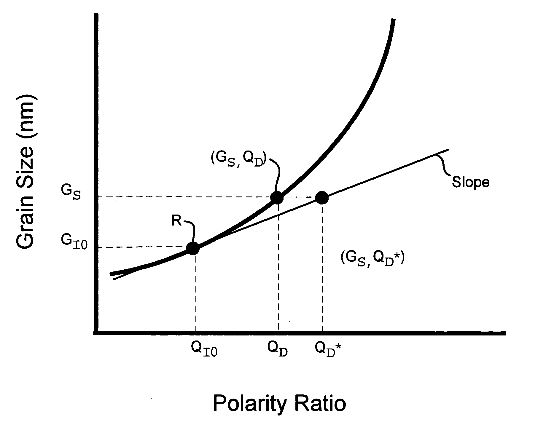
Bipolar wave current, with both positive and negative current portions, is used to electrodeposit a nanocrystalline grain size deposit. Polarity Ratio is the ratio of the absolute value of the time integrated amplitude of negative polarity current and positive polarity current. Grain size can be precisely controlled in alloys of two or more chemical components, at least one of which is a metal, and at least one of which is most electro-active. Typically, although not always, the amount of the more electro-active material is preferentially lessened in the deposit during times of negative current. The deposit also exhibits superior macroscopic quality, being relatively crack and void free. Parameters of current density, duration of pulse portions, and composition of the bath are determined with reference to constitutive relations showing grain size as a function of deposit composition, and deposit composition as a function of Polarity Ratio, or, perhaps, a single relation showing grain size as a function of Polarity ratio. A specified grain size can be achieved by selecting a corresponding Polarity Ratio, based on these relations. Coatings can be in layers, each having an average grain size, which can vary layer to layer and also in a region in a graded fashion. Coatings can be chosen for environmental protection (corrosion, abrasion), decorative properties, and for the same uses as a hard chrome coating. A finished article may be built upon a substrate of electro-conductive plastic, or metal, including steels, aluminum, brass. The substrate may remain, or be removed.

Description

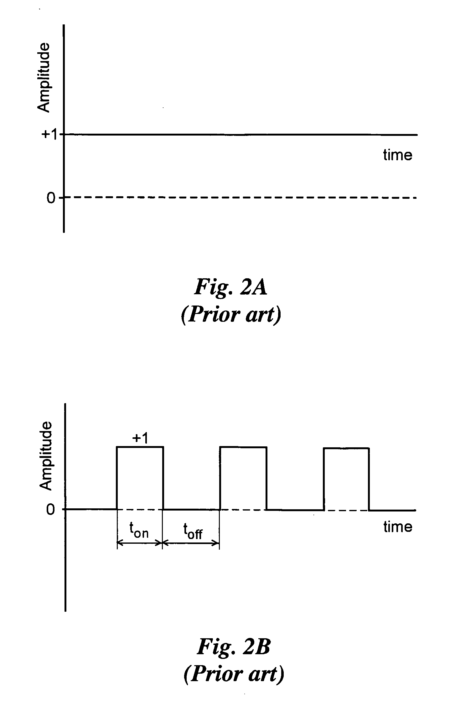
GOVERNMENT RIGHTS [0001] The United States Government has certain rights in this invention pursuant to the U.S. Army Research Office contract / grant #DAAD19-03-1-0235.[0002] A partial summary is provided below, preceding the claims. [0003] The inventions disclosed herein will be understood with regard to the following description, appended claims and accompanying drawings, where:BRIEF DESCRIPTION OF THE DRAWINGS [0004]FIG. 1 is a graphical representation showing grain size on the vertical axis as a function of liquid temperature on the horizontal axis; [0005]FIG. 2A is a schematic rendition of a direct current waveform of prior art methods of electroplating; [0006]FIG. 2B is a schematic rendition of a unipolar pulsing (UPP) current waveform of prior art methods of electroplating; [0007]FIG. 3 is a schematic representation of an apparatus invention hereof, suitable for practicing a method of an invention hereof; [0008]FIG. 4 is a schematic rendition of a scanning electron microscopy i...

Claims


Application Information

Patent Timeline
IPC IPC(8): C25D3/56
CPCC25D3/56C25D5/18Y10T428/12806Y10T428/12493Y10T428/12771C25D5/627C25D5/617C25D5/611B82Y30/00
Inventor DETOR, ANDREW J.SCHUH, CHRISTOPHER A.
Owner MASSACHUSETTS INST OF TECH
Learn More