Ferroelectric semiconductor memory device

a technology of ferroelectric semiconductors and memory devices, applied in information storage, static storage, digital storage, etc., can solve the problem of different reference levels in the first data read operation of reading out data from normal cells, and achieve the effect of reducing the number of read operations

Inactive Publication Date: 2006-11-30
PANASONIC CORP
View PDF7 Cites 7 Cited by
  • Summary
  • Abstract
  • Description
  • Claims
  • Application Information

AI Technical Summary

Benefits of technology

[0025] In one embodiment of the present invention, the control circuit varies the reference level by varying a ratio between the number of reference cells storing high-potential data and the number of reference cells storing low-potential data.
[0026] In one embodiment of the present invention, the ratio between the number of reference cells storing the high-potential data and the number of reference cells storing the low-potential data is stored in a non-volatile memory or a latch circuit, other than a ferroelectric memory element, or set by using physical or electrical fuses.
[0027] In one embodiment of the present invention, the control circuit resets all of the reference cells before accessing one or more of the large number of normal cells.
[0028] In one embodiment of the present invention, for the operation of resetting all of the reference cells before accessing the normal cells, the control circuit sets a reset time to be shorter than a data write time for the normal cells.
[0029] In one embodiment of the present invention, the control circuit does not overwrite data to the reference cell after accessing the normal cells.
[0030] In one embodiment of the present invention, the control circuit overwrites data to the reference cell after accessing the normal cells.

Problems solved by technology

However, the conventional ferroelectric semiconductor memory device has a problem in that the reference level in the first data read operation of reading out data from normal cells is different from that in the second and subsequent data read operations.

Method used


Image

  • Ferroelectric semiconductor memory device
  • Ferroelectric semiconductor memory device
  • Ferroelectric semiconductor memory device

Examples


first embodiment

[0045] A ferroelectric semiconductor memory device according to a first embodiment of the present invention will now be described.

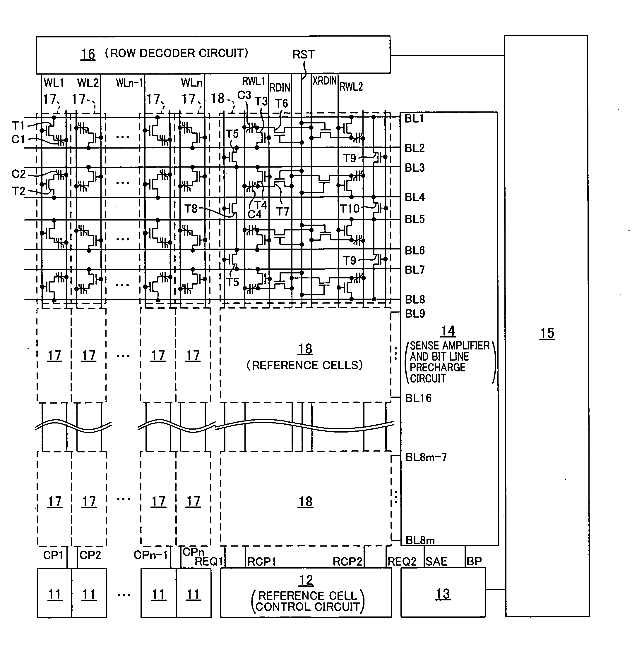
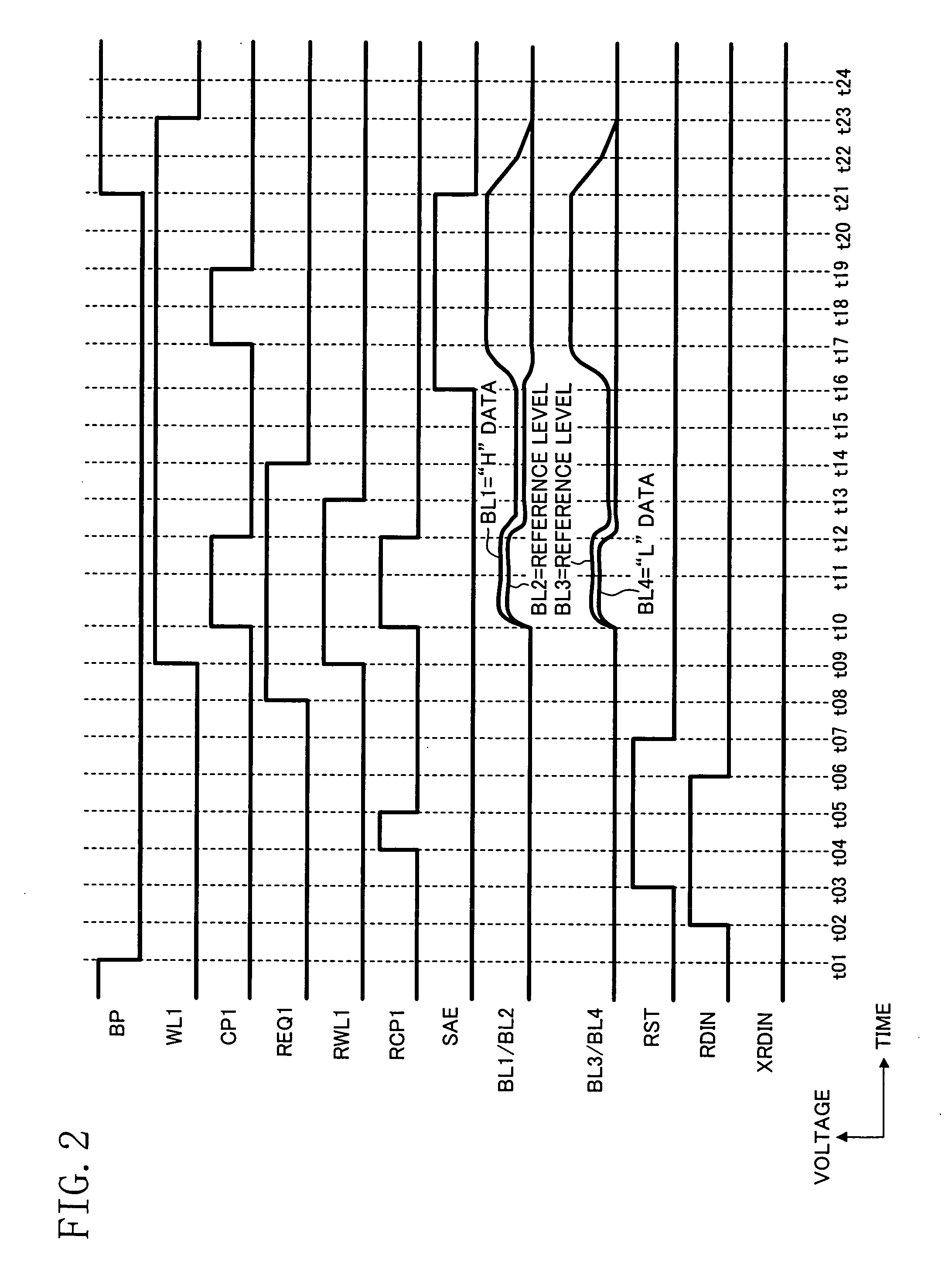
[0046]FIG. 1 shows a configuration of a memory array according to the first embodiment of the present invention. FIG. 2 is a timing diagram showing an operation according to the first embodiment of the present invention. FIGS. 3A to 3D show a trace on a hysteresis loop when reading out data from normal cells (ferroelectric memory elements) and reference cells in the reset state and in the relaxed state, and the relationship between the “H” level, the “L” level and the reference level in the reset state and in the relaxed state. FIG. 5 shows a trace on a hysteresis loop when resetting normal cells and reference cells in the relaxed state according to the first and second embodiments of the present invention. FIG. 6 shows a trace on a hysteresis loop when resetting reference cells according to the present embodiment. FIGS. 7A and 7B each schematically show...

second embodiment

[0064] A ferroelectric semiconductor memory device according to a second embodiment of the present invention will now be described with reference to the drawings.

[0065]FIG. 4 is a timing diagram showing an operation according to the second embodiment of the present invention, and FIG. 6 shows a trace on a hysteresis loop when resetting reference cells according to the present embodiment.

[0066] The ferroelectric semiconductor memory device of the present embodiment will be described with reference to FIGS. 4 and 6. The present embodiment differs from the first embodiment in that the first reference cell plate line RCP1 is at “H” in the period t17-t18 in FIG. 4. The operation until time t14 in FIG. 4 is similar to that of the first embodiment, and will not be further described below.

[0067] Part of the operation of the present embodiment that differs from the first embodiment will now be described below. The device brings the “H” data reset data RDIN to “H” at time t15 in FIG. 4, th...


PUM


Abstract

The present invention provides a ferroelectric semiconductor memory device in which the potential of data read out from a normal cell is compared with the reference level of a reference cell so as to determine whether the readout data is the “H” data or the “L” data, wherein since the reference cell is in the relaxed state when reading out data from the normal cell for the first time, the reference cell is reset before reading out data from the normal cell. Then, data is read out from the normal cell, and then the reference cell is reset. In second and subsequent data read operations of reading out data from a normal cell of another address, the reference cell is in the reset state, whereby the reference level is the same between the first data read operation and the second or subsequent data read operation. Thus, the reference level is always kept at a predetermined constant level when data is read out from normal cells.

Description

CROSS REFERENCE TO RELATED APPLICATIONS [0001] This Non-provisional application claims priority under 35 U.S.C. §119(a) on Patent Application No. 2005-160234 filed in Japan on May 31, 2005, the entire contents of which are hereby incorporated by reference. BACKGROUND OF THE INVENTION [0002] The present invention relates to a ferroelectric semiconductor memory device and, more particularly, to a technique for generating the reference level. [0003] In recent years, as the process rules becomes finer and the capacity increases, there is a shift in the type of memory cells employed in ferroelectric semiconductor memory devices, i.e., from those of a 2-transistor 2-ferroelectric capacitor type to those of a 1-transistor 1-ferroelectric capacitor type with which it is possible to realize a smaller memory size. The transistor 1-ferroelectric capacitor type requires a reference cell, in addition to a normal memory cell (hereinafter referred to as a “normal cell”), and there is increasing im...

Claims


Application Information

Patent Timeline
Patent Type & Authority Applications(United States)
IPC IPC(8): G11C11/22
CPCG11C11/22G11C7/14
Inventor YAMAOKA, KUNISATOMURAKUKI, YASUO
Owner PANASONIC CORP
Why Eureka
Try Eureka