Transistor capable of switching infrared photoelectric memory and detection functions and preparation method of transistor

An infrared light and transistor technology, applied in photovoltaic power generation, electric solid state devices, semiconductor/solid state device manufacturing, etc., can solve the problems of limited application, inability to switch infrared detection, single function, etc., to achieve improved sensitivity, short reset time, The effect of improving efficiency

Active Publication Date: 2021-02-26
UNIV OF ELECTRONICS SCI & TECH OF CHINA
View PDF10 Cites 0 Cited by
  • Summary
  • Abstract
  • Description
  • Claims
  • Application Information

AI Technical Summary

Problems solved by technology

[0004] On the basis of infrared detectors, researchers have proposed detection devices with optical memory functions, but most optical memory devices work in the visible light band, and optical memory devices in the infrared band are rarely reported. For example, in 2018, a Optical memory devices in the 1940nm band, but can only achieve infrared detection with optical memory, and cannot switch to infrared detection without optical memory (Wang Q, Wen Y, Cai K, et al.Nonvolatile infrared memory in MoS2 / PbSvan der Waals heterostructures. Science Advances, 2018, 4(4))
This detector has a single function and limited application, so it is of great significance to provide a transistor that can freely switch between the infrared light memory function and the detection function

Method used


Image

  • Transistor capable of switching infrared photoelectric memory and detection functions and preparation method of transistor
  • Transistor capable of switching infrared photoelectric memory and detection functions and preparation method of transistor
  • Transistor capable of switching infrared photoelectric memory and detection functions and preparation method of transistor

Examples


Embodiment 1

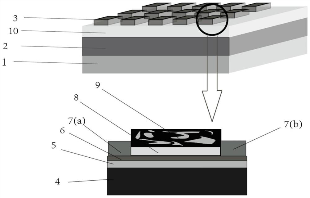
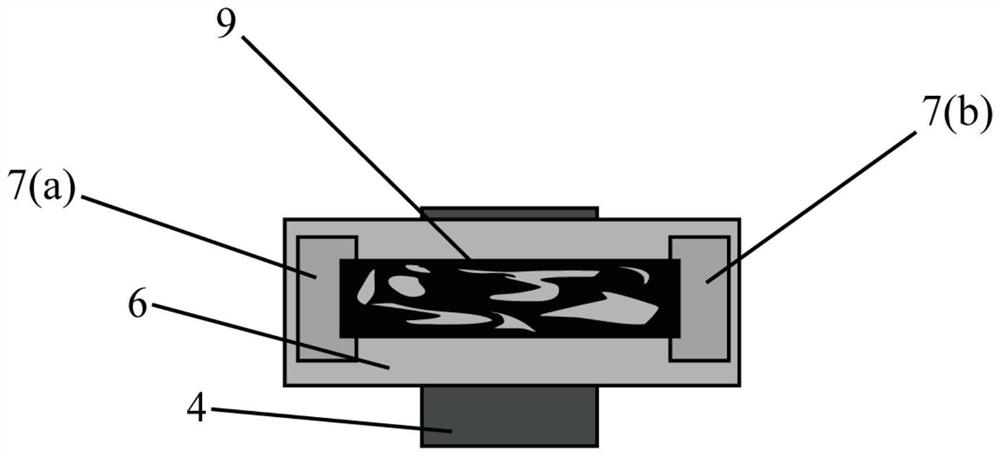
[0051] This embodiment proposes a transistor with switchable infrared photoelectric memory and detection functions, such as figure 1 , 2 As shown, it includes a silicon substrate 1, an IC circuit 2, a circuit dielectric layer 10 and a detector array 3 arranged from bottom to top; the detector array 3 is composed of a plurality of detector units arranged in an array, and the detector The detector unit includes a bottom gate electrode 4, a dielectric layer 5, graphene 6, a hole blocking layer 8 and a donor-acceptor mixed film 9 arranged from bottom to top, and the detector unit also includes a , the metal electrodes at both ends of the hole blocking layer 8, the metal electrodes include a metal drain electrode 7 (a) and a metal source electrode 7 (b), and the graphene 6 between them constitutes the graphene conductive channel of the transistor.

[0052] The silicon substrate 1 is highly doped N-type silicon; the circuit dielectric layer 10 is aluminum oxide with a thickness of ...


PUM

PropertyMeasurementUnit
thicknessaaaaaaaaaa
thicknessaaaaaaaaaa
thicknessaaaaaaaaaa

Abstract

The invention provides a transistor capable of switching infrared photoelectric memory and detection functions and a preparation method, and belongs to the technical field of optical detectors and optical energy storage. The transistor comprises a silicon substrate, an IC circuit, a circuit dielectric layer and a detector array arranged from bottom to top, wherein the detector array is composed ofa plurality of detector units arranged in an array mode; each detector unit comprises a bottom gate electrode, a dielectric layer, graphene, a hole blocking layer and a donor-acceptor mixed film which are arranged from bottom to top. The transistor further comprises metal electrodes positioned on the graphene and at two ends of the hole blocking layer. The transistor provided by the invention hasan optical memory function, and the transistor is switched among a detection mode with the optical memory, a detection mode without optical memory, a detection mode with electrical erasure optical memory and a completely closed state by adjusting the gate voltage; the transistor has potential to be applied to a switch modulator based on an infrared light communication technology and the switchingof an infrared real-time imaging function and an energy storage delay imaging function, is simple to prepare, and can be used for preparing a large-area array device.

Description

technical field [0001] The invention belongs to the technical field of optical detectors and optical energy storage, and specifically relates to a transistor capable of switching infrared photoelectric memory and detection functions and a preparation method thereof. Background technique [0002] With the development of artificial intelligence and big data in recent years, new demands have been put forward for various types of low-energy logic devices and energy storage devices with smaller sizes, and ultra-thin devices based on two-dimensional materials are expected to break the limit of Moore's theorem , becoming a potential substitute for the next generation of high-speed logic computing devices and brain-like devices. Graphene is a hexagonal lattice material with a single atomic layer, which is classified as a Dirac semimetal. Its conical zero-bandgap structure makes its energy and momentum show a linear relationship, so graphene has an ultra-high mobility (at room temper...

Claims


Application Information

Patent Timeline
Patent Type & Authority Applications(China)
IPC IPC(8): H01L27/30H01L51/42H01L51/48
CPCH10K39/32H10K30/354Y02E10/549
Inventor 杜晓扬韩嘉悦何泽宇陶斯禄王军
Owner UNIV OF ELECTRONICS SCI & TECH OF CHINA
Why Eureka
Try Eureka